Intel's new Ice Lake platform is the company's second attempt at producing a 10nm chip for the mass market, and follows on from the Cannon Lake platform. Using 'the same but different' 10nm process, Ice Lake holds inside a new 10th Gen Core microarchitecture called Sunny Cove, Gen11 graphics, and support for LPDDR4X-3733 as well as Thunderbolt and Wi-Fi 6. In advance of systems coming onto the market, Intel gave a small number of press a day of hands-on time with its Software Development Systems so we could get a taste of performance of Sunny Cove, Gen11, and Intel's newest 10nm product.
A Quick Recap on Ice Lake: Intel’s New Tick+Tock
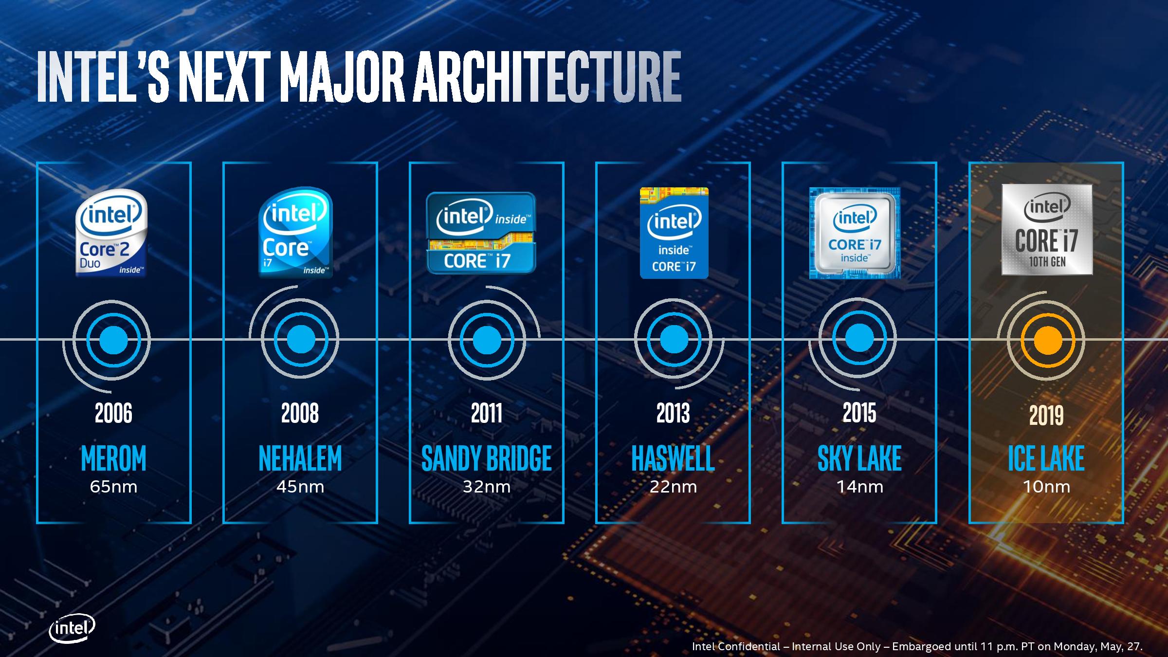
For the best part of a decade, Intel was on it’s a strategy known as Tick Tock. For every new product family and generation, it would be known as a Tick or a Tock. For any Tick, the same core design was used on a new manufacturing process node, such as moving from 45nm to 32nm. For any Tock, the same process node was used as the previous generation, but we saw a new core design and microarchitecture, such as moving from Ivy Bridge to Haswell.
Intel stayed on this Tick Tock strategy from 2006 to around 2017, when it appeared that its 10nm process node technology was to be delayed. The company moved from a two-step cadence in Tick Tock to a 3-step cadence called Process Architecture Optimization. This is essentially Tick Tock, but with another step of Optimization on the end. Unfortunately, that plan quickly unravelled, as we ended up with multiple Optimizations based on the Skylake microarchitecture built on 14nm: Kaby Lake, Kaby Lake-R, Coffee Lake, and Coffee Lake-R, not to mention the mobile space which also received Amber Lake and Whiskey Lake. Technically Intel did release a Process update in H1 2018 with Cannon Lake on 10nm, but that was a limited distribution.
The point I’m trying to make here is that Intel has historically only ever done one of two or three things with a product update: improve the process node, improve the microarchitecture, or optimize the design. Ice Lake, for the first time in a long time, sees Intel change both the process technology and the microarchitecture design at the same time. Intel has turned back the clock with a ticktock on the block.
For the general user, this is a good thing™. Not only is Ice Lake set to take advantage of new process node technology, with smaller transistor and lower voltage operation, but also apply a mélange of new features and new performance benefits at the same time. It isn’t every day we see a combined ticktock from Intel (AMD has done it twice in two years), but I’m glad it is here.
If you want to find out more on the Intel 10nm process story, please read our Cannon Lake Review.
If you want to find out more on the microarchitecture behind Sunny Cove, please read our deep dive posted earlier this week. Some finer details will be discussed in this article.
The Road to Ice Lake-U and Ice Lake-Y: 11 SKUs
Today, Intel is announcing the processors for both its Ice Lake-U and Ice Lake-Y processors. These processors are now being produced in sufficient volume to supply key launch partners with hardware in order to enable laptop and mobile designs to hit the shelves by the end of the year. Intel is not currently discussing any desktop or server processor equivalents at this time: the base Ice Lake design is current a quad-core processor with HyperThreading, and a beefy integrated graphics.

Intel’s Ice Lake SoC comes in two form factors, technically called ‘Type 3’ and ‘Type 4’. Type 3 is a bigger package, suitable for 15 W-28 W Ice Lake-U designs, while Type-4 is for 9-12 W platforms under Ice Lake-Y. Out of the processors being announced today, they mostly fall into the 9 W or 15 W categories.
| Intel 10nm Ice Lake-U Series CPUs | ||||||||
| AnandTech | Cores Threads |
Base Freq |
1C Turbo |
AC Turbo |
GPU EUs |
GPU Freq |
L3 Cache |
TDP |
| Core i7-1068G7 | 4 Cores 8 Threads |
2.3 | 4.1 | 3.6 | 64 | 1100 | 8 MB | 28 W |
| Core i7-1065G7 | 4 Cores 8 Threads |
1.3 | 3.9 | 3.5 | 64 | 1100 | 8 MB | 15 W 25 W |
| Core i5-1035G7 | 4 Cores 8 Threads |
1.2 | 3.7 | 3.3 | 64 | 1050 | 6 MB | 15 W 25 W |
| Core i5-1035G4 | 4 Cores 8 Threads |
1.1 | 3.7 | 3.3 | 48 | 1050 | 6 MB | 15 W 25 W |
| Core i5-1035G1 | 4 Cores 8 Threads |
1.0 | 3.6 | 3.3 | 32 | 1050 | 6 MB | 15 W 25 W |
| Core i3-1005G1 | 2 Cores 4 Threads |
1.2 | 3.4 | 3.4 | 32 | 900 | 4 MB | 15 W 25 W |
Sitting at the top of the stack is the Core i7-1068G7, the sole 28W processor. The name is as follows:
- Core i7 = i7 rated
- 10 = 10th Gen Core
- 6 = Position in the Stack
- 8 = 28W
- G7 = Highest Graphics (64 EUs)
For these processors, Intel is dropping the Y and the U name, and instead putting a letter and number at the end to identify how powerful the graphics are.
The Core i7-1068G7, running at a TDP of 28 W, will be the highest performing Ice Lake processor, which Intel will reserve for premium designs by its partners. We were told that partners will get it later than the others, due to the extra validation (i.e.: binning) it requires, however it does hit the 4.1 GHz that Intel has advertised as the peak frequency of the platform. The higher TDP translates in this case to a much higher base frequency than everything else (2.3 GHz rather than 1.3 GHz), and should help with maintaining turbo frequencies when not thermally limited. This processor has Iris Plus graphics, the name Intel is giving to all Gen11 graphics parts that have 48 or more EUs (so, G4 or G7).
The rest of the U series are a nominal 15 W TDP, with base frequencies from 1.0 GHz to 1.3 GHz, and turbo frequencies up to 3.9 GHz. These processors offer a cTDP up mode of 25 W, which Intel tells us won’t actually be related to any base frequency adjustment, but it will provide a higher standard of sustained turbo frequency, depending on the OEM implementation. OEMs will have to design for 25 W in order to support it.
It is worth noting that we have three versions of the Core i5-1035, all of which differ in their graphics. The G7 version has 64 execution units, the G4 has 48 execution units, and the G1 has only 32. The G4 and G1 also go slightly lower on the CPU frequency. Both the G4 and G7 graphics will be called Iris Plus, while the G1 graphics will just be called UHD Graphics.
In order to help soak up some of the lower yielding/binning U-series parts, Intel is also going to offer a dual core Core i3-1005G1.
| Intel 10nm Ice Lake-Y Series CPUs | ||||||||
| AnandTech | Cores Threads |
Base Freq |
1C Turbo |
AC Turbo |
GPU EUs |
GPU Freq |
L3 Cache |
TDP |
| Core i7-1060G7 | 4 Cores 8 Threads |
1.0 | 3.8 | 3.4 | 64 | 1100 | 8 MB | 9 W 12 W |
| Core i5-1030G7 | 4 Cores 8 Threads |
0.8 | 3.5 | 3.2 | 64 | 1050 | 6 MB | 9 W 12 W |
| Core i5-1030G4 | 4 Cores 8 Threads |
0.7 | 3.5 | 3.2 | 48 | 1050 | 6 MB | 9 W 12 W |
| Core i3-1000G4 | 2 Cores 4 Threads |
1.1 | 3.2 | 3.2 | 48 | 900 | 4 MB | 9 W 12 W |
| Core i3-1000G1 | 2 Cores 4 Threads |
1.1 | 3.2 | 3.2 | 32 | 900 | 4 MB | 9 W 12 W |
On the Y-Series, we see a similar sort of range of i7 to i3, again with G7 down to G1. The difference here is the power envelope – the nominal TDP of these processors is 9W, however a cTDP up mode for manufacturers is available at 12W.
It is also worth looking at the processor naming for the Y-Series: the ‘m3’ naming has disappeared, and so has the letter Y. If a user didn’t know any better, these parts just look like the U-series numbers. In the name, the ‘i7-1060’, that final 0 makes all the difference.
- 0 = Y-series, ~10W (9W-12W)
- 5 = U-series, 15W (or 25W in cTDP up)
- 8 = U-series, 28W
Don’t ask what Intel would name the corresponding 35W/45W H-series processors. At this point, Intel has not discussed anything higher than 28W for consumers.
Intel's Software Development System: Tested
So as you can imagine, we (the press) have been talking with Intel for so long about Ice Lake, it is getting to a point where we’re just asking if it is ready yet. Earlier in the year, I floated an idea to Intel that basically said this:
“When you are ready with a reference design for your partners, let us test it. It’s not an optimized design, but it will have the raw performance that your partners aim to beat, and provide a good base line to drum up potential interest.”
My reference point for these discussions was what Qualcomm does on the smartphone side. For multiple generations, Qualcomm has invited select press to come test its ‘Qualcomm Reference Design’ (QRD) models for its latest smartphone chipsets. It provides a preview of the performance, and we see Qualcomm’s partners either optimize it like crazy for better performance, or produce radically unique thin form factor designs to provide the best in-hand experience while still being competitive in performance and thermals.
- The Snapdragon 855 Performance Preview: Setting the Stage for Flagship Android 2019
- The Snapdragon 845 Performance Preview: Setting the Stage for Flagship Android 2018
- The Qualcomm Snapdragon 835 Performance Preview
Well it appears that someone at Intel thought it was a good idea. The group of new employees that Intel has hired from the press side of the fence over the last year or so floated the idea up the chain, and have made it happen. We got to test Ice Lake before systems are on the shelves.
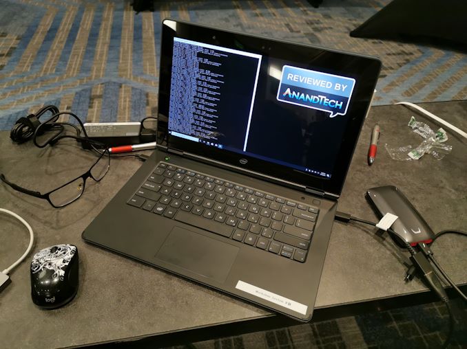
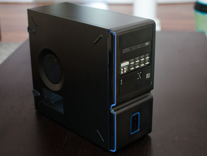
What Intel provided us was a day of testing in a conference room close to HQ in Santa Clara. These machines were Software Development Systems, or SDS laptops, that go out to Intel’s software partners like Adobe and Microsoft for functional testing.
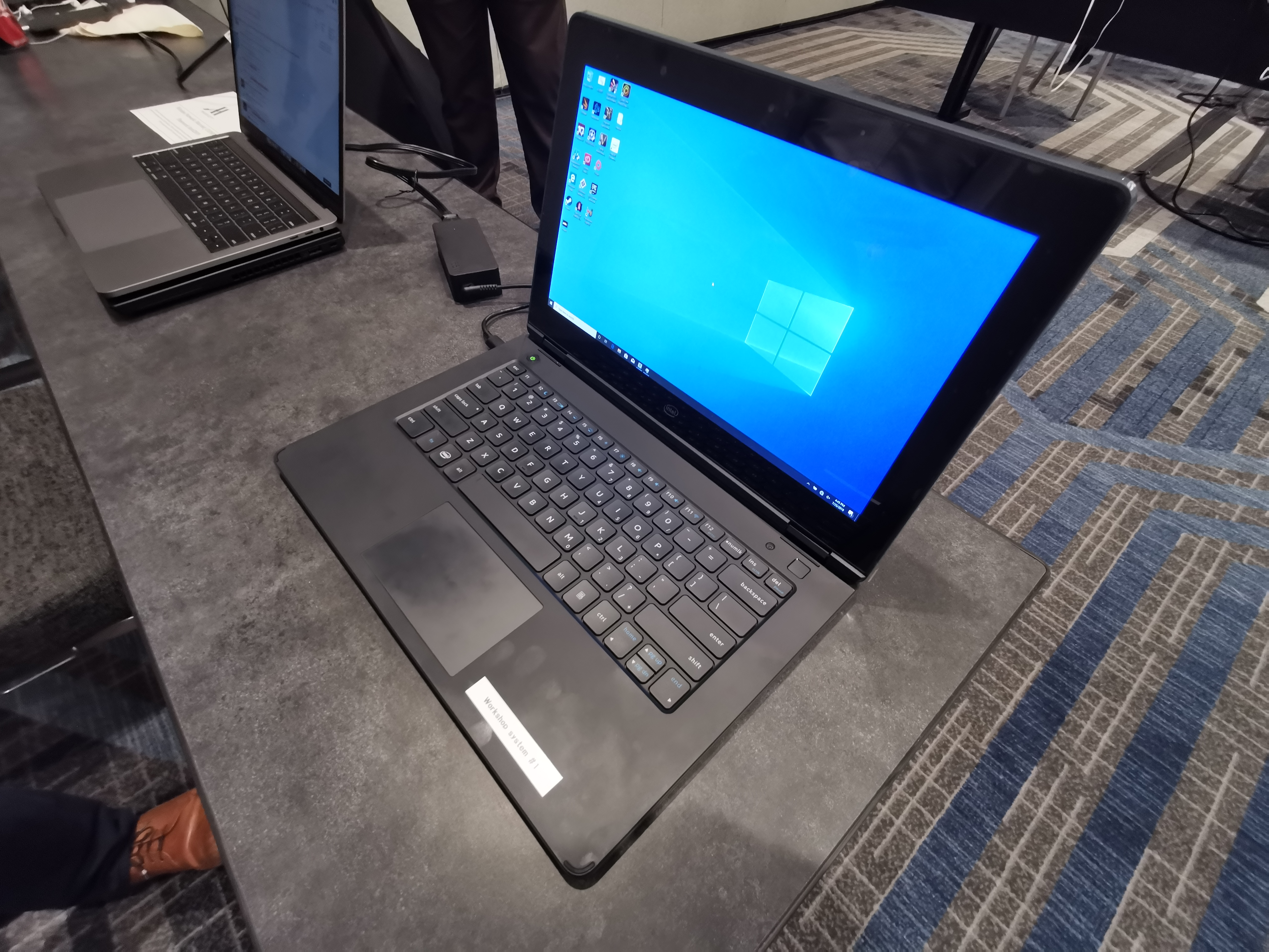
Like other reference designs (such as Qualcomm’s), these units are designed to work, and are for the best part thermally unconstrained. The fan is on all the time, there are massive bezels, and the device itself is a bit chunky, to provide all the ports that the chip can provide. Ultimately OEMs can take these reference designs and add/remove components as they see fit, or use it as a guide to build their own from the ground up. These SDS platforms are clearly based on the Lenovo Yoga series, given the hinge mechanism and the Lenovo power bricks, but that makes sense that Intel might partner with one of its closest allies in order to produce a run of these systems.

As always with testing reference design machines, there are a few caveats worth mentioning.
- Units to stay in the room being tested (a hotel conference room near Intel HQ)
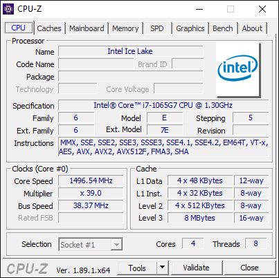
- These systems are Core i7-1065G7 units, running in 15W mode.
- Intel enabled an option so we could choose to run them in a 25W configuration.
- Intel NVMe 256GB SSD, Four Thunderbolt 3 ports, 2x4GB LPDDR4X-3733 DRAM
- The fan is on 100%
- Intel pre-installed Windows 10 Pro 1903, Build 18362.239, with ICL chipset and graphics drivers
- We were not allowed to change the OS. We could request an image reset. This was because the 15W/25W mode was a special config, plus the drivers were still beta and not wrapped in suitable installers yet
- It came with pre-installed benchmarks. We could remove these (I did).
- No thermal or battery life testing, as these units are just functional demos.
- Power testing was OK.
- Can run and install any benchmark, as long as it didn’t ‘phone home’ (to stop leaks).
- Total testing time, ~8 hours
Now to be honest, most of these from my point of view were to be expected. Only test the device in a specific location for a limited time, with no thermal/battery life on a development system. I was ok with that. Being OS limited, and having preinstalled benchmarks, was a bit awkward. I discussed this internally with other AnandTech editors, and we had differing opinions (from ‘as expected’ to ‘this could lead to cheating’).
After attending the event, to which fewer than 10 press were invited, I now understand why. Some of the press invited didn’t have OS images, didn’t bring benchmarks with them, and were quite happy to go along with the flow. Intel provided benchmarks like Geekbench and 3DMark, which those press with their audiences were happy to run. I came prepared with both a new 1903 OS image and my benchmark suite, ready to rock and roll.
What We Tested
There are two ways to approach this sort of limited time testing environment, and it was clear which of the press in attendance were going for which audience. There is device and performance testing, which aims to show how a device might perform in tests with a standard user, and there is functional testing, getting to the heart of the new microarchitecture and what it can do. We did a little of column A, but mostly column B.
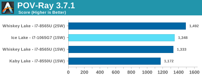
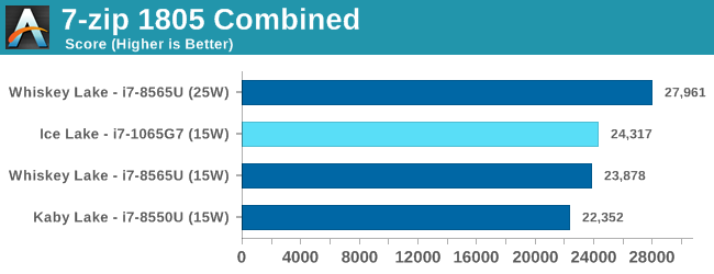
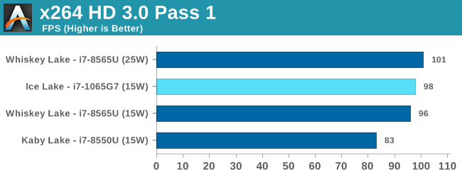
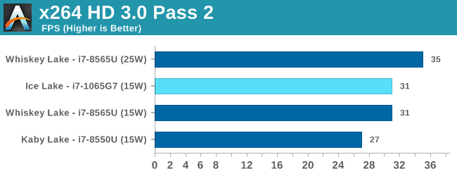
Our comparison points for this test are two Huawei laptops: a Matebook 13 2019 with a Whiskey Lake i7-8565U and 8GB of DDR4-3200, and a Matebook X Pro 2018, with a Kaby Lake-R Core i7-8500U. Both of these are quad-core CPUs with a nominal TDP of 15W (the X Pro might be running in 25W mode due to its design, however). We also have dual core results from our Core i3-8121U Cannon Lake 15W laptop, a Core i3-8130U Kaby Lake-R mini-PC, and some other low powered CPUs.
| Intel Core i7-1065G7 Comparison | |||||
| Core i7-1065G7 |
AnandTech | Core i7-8565U |
Core i7-8550U |
Core i3-8130U |
Core i3-8121U |
| 10+ | Process | 14++ | 14+ | 14+ | 10 |
| Sunny Cove | uArch | Whiskey Lake | Kaby Lake-R | Kaby Lake | Cannon Lake |
| 4C / 8T | Cores | 4C / 8T | 4C / 8T | 2C / 4T | 2C / 4T |
| 1.3 GHz | Base Freq | 1.8 GHz | 1.8 GHz | 2.2 GHz | 2.2 GHz |
| 3.9 GHz | 1C Turbo | 4.6 GHz | 4.0 GHz | 3.4 GHz | 3.2 GHz |
| Gen11 | GPU uArch | Gen9.5 | Gen9.5 | Gen9.5 | - |
| 64 | GPU EUs | 24 | 24 | 24 | - |
| 1.10 GHz | GPU Freq | 1.15 GHz | 1.15 GHz | 1.00 GHz | - |
| AVX-512 | AVX | AVX2 | AVX2 | AVX2 | AVX-512 |
| 15 W | TDP | 15 W | 15 W | 15 W | 15 W |
| 2x 4GB LPDDR4X 3733 |
DRAM | 2x 4GB LPDDR3 2133 |
2x 8GB LPDDR3 2133 |
2x 4GB DDR4 2400 |
2x 4GB DDR4 2400 |
Ideally we would have tested with an AMD Ryzen 3700U in the mix as well, but unfortuantely samples of those systems seem to be rather rare. We understand that testing against AMD should be part of this analysis, but none of AMD's partners have sent us a new AMD system to test in quite a while.
With our benchmark selection, given what we wanted to test, we were actually pretty limited because a couple of our key tests actually take a number of hours. Our time breakdown started from this:
- Copy Benchmarks from USB 3.0 drive, 0h25m
- Installing benchmarks from scripts, 0h40m
- Running instruction verification tests, 0h35m
- SPEC 2006, 2h00m
- SPEC 2007, 2h20m
- Power Testing, 0h20m
That gave me 2h40m left. In that time we ran some of our regular benchmark suite, just a few tests, and then three quick game titles with our IGP settings. We tested everything at 15W, except our game tests and power tests, which we also ran in 25W mode. Unfortunately we ran out of time to do anything more.
Ideally I need another couple of days with the system. But this is what system testing is like, even with benchmarks prepared and ready to go, especially if you want to find out all the intricacies of a new architecture.
Read on for a report into our testing.
One of the biggest changes in the new Sunny Cove core is the cache hierarchy. Throughout most of the last decade, Intel has kept the same cache configuration among its server cores with very few changes, aside from improving the micro-op cache through Sandy Bridge today, but with Sunny Cove, we get some key updates.
From our microarchitecture disclosure article, we know that Sunny Cove brings with it an increased L1 data cache, as well as a doubled L2 cache, from Skylake. With this comes more associativity as well.
| Core Cache Comparison | ||||||
| Sunny Cove |
AnandTech | Cannon Lake |
Skylake | Sandy Bridge |
AMD Zen 2 |
|
| 48 KB 12-way |
L1-D | 32 KB 8-way |
32 KB 8-way |
32 KB 8-way |
32 KB 8-way |
|
| 32 KB 8-way |
L1-I | 32 KB 8-way |
32 KB 8-way |
32 KB 8-way |
32 KB 8-way |
|
| 512 KB 8-way |
L2 | 256 KB 4-way |
256 KB 4-way |
256 KB 8-way |
512 KB 8-way |
|
| 2 MB 16-way |
L3/core | 2 MB 16-way |
2 MB 16-way |
2MB 16-way |
4 MB 16-way |
|
| 2304 | uOp Cache | 1536 | 1536 | 1536 | 4096 | |
I’ve also included the size of the micro-op cache in this comparison, because we understand that the L1-D and the micro-op cache are typically located next to each other in the die design – increasing the size of one typically means limiting the size of the other, however given that both of them work to accelerate the same types of data, it is important to find the right balance: AMD for Zen 2 decided to halve the L1-D, double increase the L1-D associativity, and then double the micro-op cache from 2k to 4k entries. For Sunny Cove, Intel has increased the L1-D by 50%, but also increased the micro-op cache by 50%, taking advantage of the second generation 10nm process.
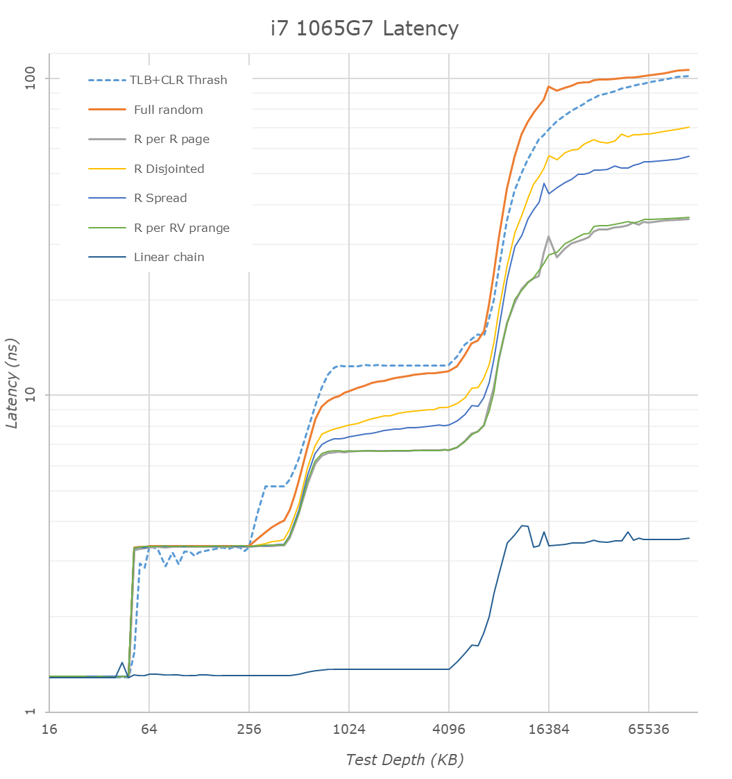
In the above latency graph comparison, we can notably see the new increased cache capacities. The L1’s increase from 32KB to 48KB is well visible, as well as the L2 increase from 256KB to 512KB.
On the part of the L2 it’s interesting to see that again the new core’s TLB structures don’t quite cover the whole capacity of the L2 and that’s why the latter half of the L2 has worse access latencies for L1D TLB miss patterns.
L3 latencies look similar, however we’ll dwell into that just in a bit. The DRAM latencies of course are apples and oranges in this case as Intel’s new LPPDR4X memory controller in the new ICL part doesn’t have a counter-part we can compare to, but as expected the memory latency is notably worse than a desktop part so no big surprises there.
What’s rather disappointing however is that we’re not really seeing any kind of change to the prefetchers and our access patterns between the two microarchitectures look identical. We had expected Intel to improve in this regard, but alas it seems, at least for our test cases, there’s been no improvements.
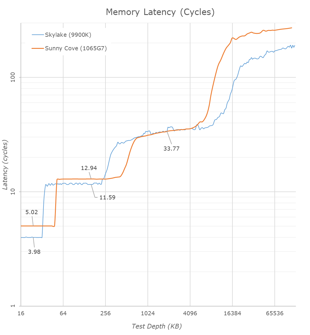
One of the major balancing acts with cache sizes is also cache latency. The bigger the cache, the longer it takes to retrieve data from it – increasing associativity can do this as well. Intel for the longest time has cited a 4-cycle latency to its L1 cache, and a 12-cycle latency to its L2 cache. This changes, in quite a substantial way.
| Core Cache Latency (in cycles) | ||||||
| Sunny Cove | AnandTech | Cannon Lake |
Skylake | Sandy Bridge |
AMD Zen 2 |
|
| 5 | L1 | 4 | 4 | 4 | 4 | |
| 13 | L2 | 12 | ~12 | 12 | 12 | |
| 30-36 | L3 | 26-37 | 34 | |||
Due to the increase in the L1 cache, that 4-cycle latency is now a 5-cycle latency. Intel is hoping that its double L1 store bandwidth will help hide that latency, however adding 20% latency onto every data fetch is a heavy hit to take. This is why a lot of the rest of the core is also beefed up, so work can still continue to cover for this extra cycle. It is worth noting that Intel’s Atom cores in the past had an L1 latency of 3 cycles, however they have also since moved to 4-cycle.
The L2 also changes, from 12 cycles to 13 cycles. You can’t double a cache for free, and it is interesting to note here that now AMD and Intel share the same L2 cache size and the same associativity, however AMD has a cycle advantage on Intel. This has a knock on effect for L3 cache latency too, which has increased from ~26-37 cycles to ~30-36 cycles on Intel, from Skylake. The latency here isn’t uniform because the cache isn’t uniform, and accessing non-local L3 slices comes with a latency penalty, as say opposed to AMD’s uniform latency L3.
One of the biggest additions Intel was keen to make in our Sunny Cove microarchitecture disclosure is the increase in the L1 bandwidth. Based on our testing, Skylake’s L1 data cache was capable of 2x32-byte read and 1x32-byte write per clock. For Sunny Cove this has increased, but it gets a bit more complicated. In one clock Sunny cove can perform 2x64-byte reads and either 1x64-byte write, or 1x32-byte write, or 2x16-byte writes. So both reads and writes, at peak, have doubled with bit width, with the write configurations being a bit more complex.

We can see the direct effects of the bandwidth change in our bandwidth tests. The L1 store bandwidth is extremely evident as it measures in at 222GB/s on the ICL part, while only reaching 139GB/s on the 28% higher clocked 9900K. If we normalise for frequency, we indeed see a doubling of the store bandwidth of the new core.
The L2 cache bandwidth looks unchanged from Skylake – the part here lags behind with an equal amount to the frequency difference. Surprisingly, the L3 bandwidth fares quite well here and is almost at parity to the desktop 9900K even though the frequency difference. The DRAM bandwidth is inferior on the ICL mobile chip, but again that’s to be expected due to the apples and oranges DRAM architecture comparison.
Moving on to the TLB configurations, and it turns out that Intel has moved where this data is stored. This data is typically stored in CPUID.02h, however it is now found in CPUID.18h, and the info between different page sizes and capabilities is now given as subdivisions. The TLBs look as follows, and broken down into configurations:
| Sunny Cove TLB | |||
| AnandTech | Type | Entries | Associativity |
| L1-D | 4K | 64 | 4-way |
| L1-D | 2M | 32 | 4-way |
| L1-D | 1G | 8 | full |
| L1-I | 4K+2M | 8 | full |
| L1-I | 4K+2M+1G | 16 | full |
| L2 | 4K+2M | 1024 | 8-way |
| L2 | 4K+1G | 1024 | 8-way |
This means that for 4K and 2M L1-I entries, there are a total 8+16 = 24 possible, but only 16 1G possible. For 4K L2 entries, there are 1024 + 1024 = 2048 entries possible, however only 1024 each of 2M/1G are possible. The peak numbers align with what Intel has told us in our microarchitecture disclosure, however it is good to dive into what is possible.
With every new microarchitecture update, there are goals on several fronts: add new instructions, decrease the latency of current instructions, increase the throughput of current instructions, and remove bugs. The big headline addition for Sunny Cove and Ice Lake is AVX-512, which hasn’t yet appeared on a mainstream widely distributed consumer processor – technically we saw it in Cannon Lake, but that was a limited run CPU. Nonetheless, a lot of what went into Cannon Lake also shows up in the Sunny Cove design. To complicate matters, AVX-512 comes in plenty of different flavors. But on top of that, Intel also made a significant number of improvements to a number of instructions throughout the design.
Big thanks to InstLatX64 for his help in analyzing the benchmark results.
Security
On security, almost all the documented hardware security fixes are in place with Sunny Cove. Through the CPUID results, we can determine that SSBD is enabled, as is IA32_ARCH_CAPABILITIES, L1D_FLUSH, STIBP, IBPB/IBRS and MD_CLEAR.
This aligns with Intel’s list of Sunny Cove security improvements:
| Sunny Cove Security | |||
| AnandTech | Description | Name | Solution |
| BCB | Bound Check Bypass | Spectre V1 | Software |
| BTI | Branch Target Injection | Spectre V2 | Hardware+OS |
| RDCL | Rogue Data Cache Load | V3 | Hardware |
| RSSR | Rogue System Register Read | V3a | Hardware |
| SSB | Speculative Store Bypass | V4 | Hardware+OS |
| L1TF | Level 1 Terminal Fault | Foreshadow | Hardware |
| MFBDS | uArch Fill Buffer Data Sampling | RIDL | Hardware |
| MSBDS | uArch Store Buffer Data Sampling | Fallout | Hardware |
| MLPDS | uArch Load Port Data Sampling | - | Hardware |
| MDSUM | uArch Data Sampling Uncachable Memory | - | Hardware |
Aside from Spectre V1, which has no suitable hardware solution, almost all of the rest have been solved through hardware/firmware (Intel won’t distinguish which, but to a certain extent it doesn’t matter for new hardware). This is a step in the right direction, but of course it may have a knock-on effect, plus for anything that gets performance improvements being moved from firmware to hardware will be rolled into any advertised IPC increase.
Also on the security side is SGX, or Intel’s Software Guard Instructions. Sunny Cove now becomes Intel’s first public processor to enable both AVX-512 and SGX in the same design. Technically the first chip with both SGX and AVX-512 should have been Skylake-X, however that feature was ultimately disabled due to failing some test validation cases. But it now comes together for Sunny Cove in Ice Lake-U, which is also a consumer processor.
Instruction Improvements and AVX-512
As mentioned, Sunny Cove pulls a number of key improvements from the Cannon Lake design, despite the Cannon Lake chip having the same cache configuration as Skylake. One of the key points here is the 64-bit division throughput, which goes from a 97-cycle latency to an 18-cycle latency, blowing past AMD’s 45-cycle latency. As an ex-researcher with no idea about instruction latency or compiler options, working on high-precision math code, this speedup would have been critical.
- IDIV -> 97-cycle to 18-cycle
For the general purpose registers, we see a lot of changes, and most of them quite sizable.
| Sunny Cove GPR Changes | |||
| AnandTech | Instruction | Skylake | Sunny Cove |
| Complex LEA | Complex Load Effective Address | 3 cycle latency 1 per cycle |
1 cycle latency 2 per cycle |
| SHL/SHR | Shift Left/Right | 2 cycle latency 0.5 per cycle |
1 cycle latency 1 per cycle |
| ROL/ROR | Rotate Left/Right | 2 cycle latency 0.5 per cycle |
1 cycle latency 1 per cycle |
| SHLD/SHRD | Double Precision Shift Left/Right | 4 cycle latency 0.5 per cycle |
4 cycle latency 1 per cycle |
| 4*MOV | Four repated string MOVS | Limited instructions | 104 bits/clock All MOVS* Instructions |
In the past we’ve seen x87 instructions being regressed, made slower, as they become obsolete. For whatever reason, Sunny Cove decreases the FMUL latency from 5 cycles to 4 cycles.
The SIMD units also go through some changes:
| Sunny Cove SIMD | |||
| AnandTech | Instruction | Skylake | Sunny Cove |
| SIMD Packing | SIMD Packing now slower | 1 cycle latency 1 per cycle |
3 cycle latency 1 per cycle |
| AES* | AES Crypto Instructions (for 128-bit / 256-bit) |
4 cycle latency 2 per cycle |
3 cycle latency 2 per cycle |
| CLMUL | Carry-Less Multiplication | 7 cycle latency 1 per cycle |
6 cycle latency 1 per cycle |
| PHADD/PHSUB | Packed Horizontal Add/Subtract and Saturate |
3 cycle latency 0.5 per cycle |
2 cycle latency 1 per cycle |
| VPMOV* xmm | Vector Packed Move | 2 cycle latency 0.5 per cycle |
2 cycle latency 1 per cycle |
| VPMOV* ymm | Vector Packed Move | 4 cycle latency 0.5 per cycle |
2 cycle latency 1 per cycle |
| VPMOVZX/SX* xmm | Vector Packed Move | 1 cycle latency 1 per cycle |
1 cycle latency 2 per cycle |
| POPCNT | Microcode 50% faster than SW (under L1-D size) | ||
| REP STOS* | Repeated Store String | 62 bits/cycle | 54 bits/cycle |
| VPCONFLICT | Still Microcode Only | ||
We’ve already gone through all of the new AVX-512 instructions in our Sunny Cove microarchitecture disclosure. These include the following families:
- AVX-512_VNNI (Vector Neural Network Instructions)
- AVX-512_VBMI (Vector Byte Manipulation Instructions)
- AVX-512_VBMI2 (second level VBMI)
- AVX-512_ BITALG (bit algorithms)
- AVX-512_IFMA (Integer Fused Multiply Add)
- AVX-512_VAES (Vector AES)
- AVX-512_VPCLMULQDQ (Carry-Less Multiplacation of Long Quad Words)
- AVX-512+GFNI (Galois Field New Instructions)
- SHA (not AVX-512, but still new)
- GNA (Gaussian Neural Accelerator)
(Intel also has the GMM (Gaussian Mixture Model) inside the core since Skylake, but I’ve yet to see any information on this outside a single line in the coding manual.)
For all these new AVX-512 instructions, it’s worth noting that they can be run in 128-bit, 256-bit, or 512-bit mode, depending on the data types passed to it. Each of these can have corresponding latencies and throughputs, which often get worse when going for the 512-bit mode, but overall assuming you can fill the register with a 512-bit data type, then the overall raw processing will be faster, even with the frequency differential. This doesn’t take into account any additional overhead for entering the 512-bit power state, it should be noted.
Most of these new instructions are relatively fast, with most of them only 1-3 cycles of latency. We observed the following:
| Sunny Cove Vector Instructions | |||||
| AnandTech | Instruction | XMM | YMM | ZMM | |
| VNNI | Latency | Vector Neural Network Instructions | 5-cycle | 5-cycle | 5-cycle |
| Throughput | 2/cycle | 2/cycle | 1/cycle | ||
| VPOPCNT* | Latency | Return the number of bits set to 1 | 3-cycle | 3-cycle | 3-cycle |
| Throughput | 1/cycle | 1/cycle | 1/cycle | ||
| VPCOMPRESS* | Latency | Store Packed Data | 3-cycle | 3-cycle | 3-cycle |
| Throughput | 0.5/cycle | 0.5/cycle | 0.5/cycle | ||
| VPEXPAND* | Latency | Load Packed Data | 5-cycle | 5-cycle | 5-cycle |
| Throughput | 0.5/cycle | 0.5/cycle | 0.5/cycle | ||
| VPSHLD* | Latency | Vector Shift | 1-cycle | 1-cycle | 1-cycle |
| Throughput | 2/cycle | 2/cycle | 1/cycle | ||
| VAES* | Latency | Vector AES Instructions | 3-cycle | 3-cycle | 3-cycle |
| Throughput | 2/cycle | 2/cycle | 1/cycle | ||
| VPCLMUL | Latency | Vector Carry-Less Multiply | 6-cycle | 8-cycle | 8-cycle |
| Throughput | 1/cycle | 0.5/cycle | 0.5/cycle | ||
| GFNI | Latency | Galois Field New Instructions | 3-cycle | 3-cycle | 3-cycle |
| Throughput | 2/cycle | 2/cycle | 1/cycle | ||
For all of the common AVX2 instructions, xmm/ymm latencies and throughputs are identical to Skylake, however zmm is often a few cycles slower for DIV/SQRT variants.
Other Noticeable Observations
From our testing, we were also able to prove some of the other parts of the core, such as the added store ports and shuffle units.
Our data shows that the second store port is not identical to the first, which explains the imbalance when it comes to writes: rather than supporting 2x64-bit with loads, it only supports either 1x64-bit write, or 1x32-bit write, or 2x16-bit writes. This means we mainly see speed ups with GPR/XMM data, and the result is only a small improvement for 512-bit SCATTER instructions. Otherwise, it seems not to work with any 256-bit or 512-bit operand (you can however use it with 64-bit AVX-512 mask registers). This is going to cause a slight headache for anyone currently limited by SCATTER stores.
The new shuffle unit is only 256-bit wide. It will handle a number of integer instructions (UNPCK, PSLLDQ, SHUF*, MOVSHDUP, but not PALIGNR or PACK), but only a couple of floating point instructions (SHUFPD, SHUFPS).
Section by Andrei Frumusanu
SPEC2017 and SPEC2006 is a series of standardized tests used to probe the overall performance between different systems, different architectures, different microarchitectures, and setups. The code has to be compiled, and then the results can be submitted to an online database for comparsion. It covers a range of integer and floating point workloads, and can be very optimized for each CPU, so it is important to check how the benchmarks are being compiled and run.
We run the tests in a harness built through Windows Subsystem for Linux, developed by our own Andrei Frumusanu. WSL has some odd quirks, with one test not running due to a WSL fixed stack size, but for like-for-like testing is good enough. SPEC2006 is deprecated in favor of 2017, but remains an interesting comparison point in our data. Because our scores aren’t official submissions, as per SPEC guidelines we have to declare them as internal estimates from our part.
For compilers, we use LLVM both for C/C++ and Fortan tests, and for Fortran we’re using the Flang compiler. The rationale of using LLVM over GCC is better cross-platform comparisons to platforms that have only have LLVM support and future articles where we’ll investigate this aspect more. We’re not considering closed-sourced compilers such as MSVC or ICC.
clang version 8.0.0-svn350067-1~exp1+0~20181226174230.701~1.gbp6019f2 (trunk)
clang version 7.0.1 (ssh://git@github.com/flang-compiler/flang-driver.git
24bd54da5c41af04838bbe7b68f830840d47fc03)-Ofast -fomit-frame-pointer
-march=x86-64
-mtune=core-avx2
-mfma -mavx -mavx2
Our compiler flags are straightforward, with basic –Ofast and relevant ISA switches to allow for AVX2 instructions. Despite ICL supporting AVX-512, we have not currently implemented it, as it requires a much greater level of finesse with instruction packing. The best AVX-512 software uses hand-crafted intrinsics to provide the instructions, as per our 3PDM AVX-512 test later in the review.
For these comparisons, we will be picking out CPUs from across our dataset to provide context. Some of these might be higher power processors, it should be noted.
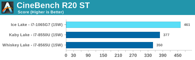
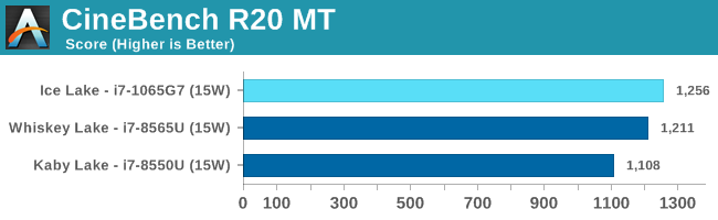
SPECint2006
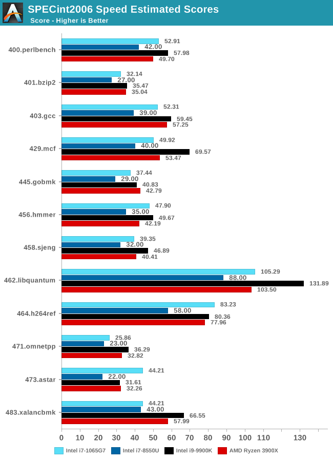
Amongst SPECint2006, the one benchmark that really stands out beyond all the rest is the 473.astar. Here the new Sunny Cove core is showcasing some exceptional IPC gains, nearly doubling the performance over the 8550U even though it’s clocked 100MHz lower. The benchmark is extremely branch misprediction sensitive, and the only conclusion we can get to rationalise this increase is that the new branch predictors on Sunny Cove are doing an outstanding job and represent a massive improvement over Skylake.
456.hmmer and 464.h264ref are very execution bound and have the highest actual instructions per clock metrics in this suite. Here it’s very possible that Sunny Cove’s vastly increased out-of-order window is able to extract a lot more ILP out of the program and thus gain significant increases in IPC. It’s impressive that the 3.9GHz core here manages to match and outpace the 9900K’s 5GHz Skylake core.
Other benchmarks here which are limited by other µarch characteristics have various increases depending on the workload. Sunny Cove doubled L2 cache should certainly help with workloads like 403.gcc and others. However because we’re also memory latency limited on this platform the increases aren’t quite as large as we’d expect from a desktop variant of ICL.
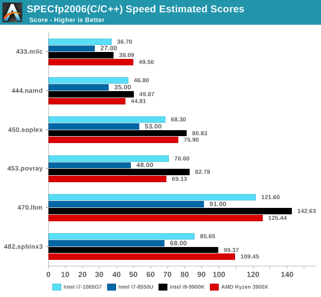
In SPECfp2006, Sunny Cove’s wider out-of-order window can again be seen in tests such as 453.povray as the core is posting some impressive gains over the 8550U at similar clocks. 470.lbm is also instruction window as well as data store heavy – the core’s doubled store bandwidth here certainly helps it.
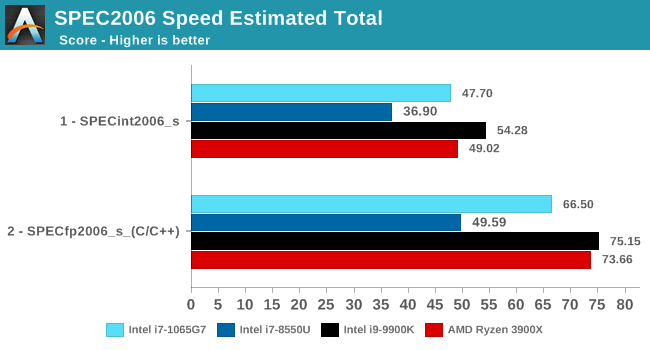
Overall in SPEC2006, the new i7-1065G7 beats a similarly clocked i7-8550U by a hefty 29% in the int suite and 34% in the fp suite. Of course this performance gap will be a lot smaller against 9th gen mobile H-parts at higher clocks, but these are also higher TDP products.
The 1065G7 comes quite close to the fastest desktop parts, however it’s likely it’ll need a desktop memory subsystem in order to catch up in total peak absolute performance.
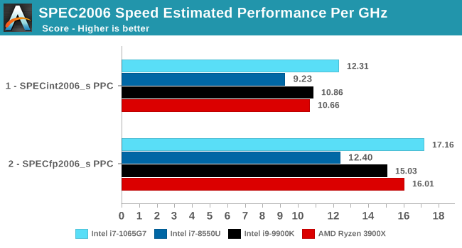
Performance per clock increases on the new Sunny Cove architecture are outstandingly good. IPC increases against the mobile Skylake are 33 and 38% in the integer and fp suites, though we also have to keep in d mind these figures go beyond just the Sunny Cove architecture and also include improvements through the new LPDDR4X memory controllers.
Against a 9900K, although apples and oranges, we’re seeing 13% and 14% IPC increases. These figures likely would be higher on an eventual desktop Sunny Cove part.
SPEC2017
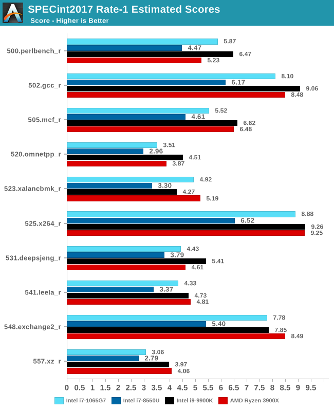
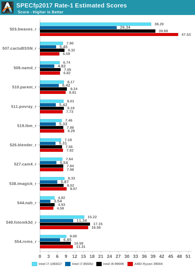
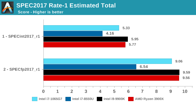
The SPEC2017 results look similar to the 2006 ones. Against the 8550U, we’re seeing grand performance uplifts, just shy of the best desktop processors.
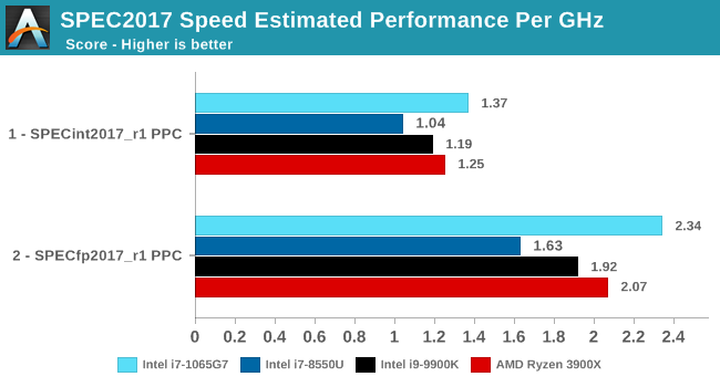
Here the IPC increase also look extremely solid. In the SPECin2017 suite the Ice Lake part achieves a 14% increase over the 9900K, however we also see a very impressive 21% increase in the fp suite.
Overall in the 2017 suite, we’re seeing a 19% increase in IPC over the 9900K, which roughly matches Intel’s advertised metric of 18% IPC increase.
Based on the SKU table, Intel was very keen to point out that all of the Y-series processors for Ice Lake and all the 15W U-series processors have cTDP up modes. This means that OEMs, if they build for it, can take advantage of a higher base power of a processor which leads to longer turbo periods and a higher frequency during sustained performance levels.
While cTDP is a good idea, one of the issues we have with the concept is that Intel’s OEM partners that design the laptops and notebooks for these processors don’t ever advertise or publicise if they’re using a CPU in cTDP up or down mode. I could understand why a vendor might not want to advertise using a down mode, but an up mode means extra performance, and it’s hard to tell from the outside what is going on.
For what it is worth, most users cannot change between these modes anyway. They are baked into the firmware and the operating system. However there are a few systems that do expose this to the user, as I recently found out with my Whiskey Lake-U platform, where the OS power plan has advanced options to set the TDP levels. Very interesting indeed.
Also, for Ice Lake-U, Intel is introducing a feature called Intel Dynamic Tuning 2.0.
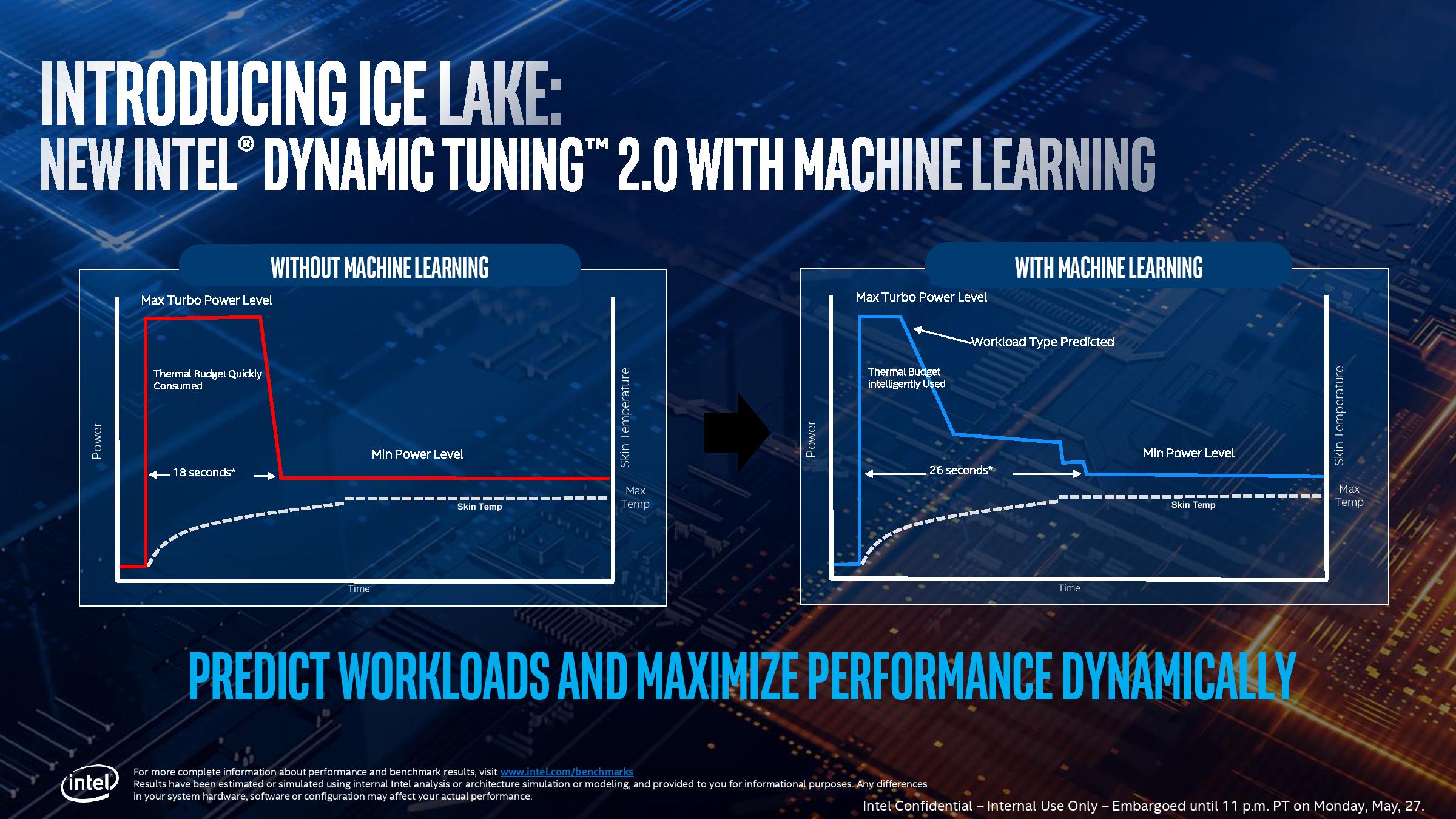
We covered this in our architecture disclosure article, but the short and simple of it is that it allows OEMs to implement a system whereby the PL1/TDP of a system can change based on an algorithm over time. So it allows for higher strict turbo, and then adjusts the turbo budget over time.
This feature will be branded under Intel’s Adaptix brand, which covers all these CPU optimizations. However, it should be noted, that this feature is optional for the OEM. It requires the OEM to actually do the work to characterize the thermal profile of the system. We suspect that it will be mostly on premium devices, but as the chips roll out into cheaper systems, this will not be there. Intel is not making this feature standard.
Testing Power
Based on the time available, we weren’t able to do much power testing. What I was able to do was run a power profile during the start of our 3DPM AVX512 test in both 15W and 25W modes for the Core i7-1065G7.
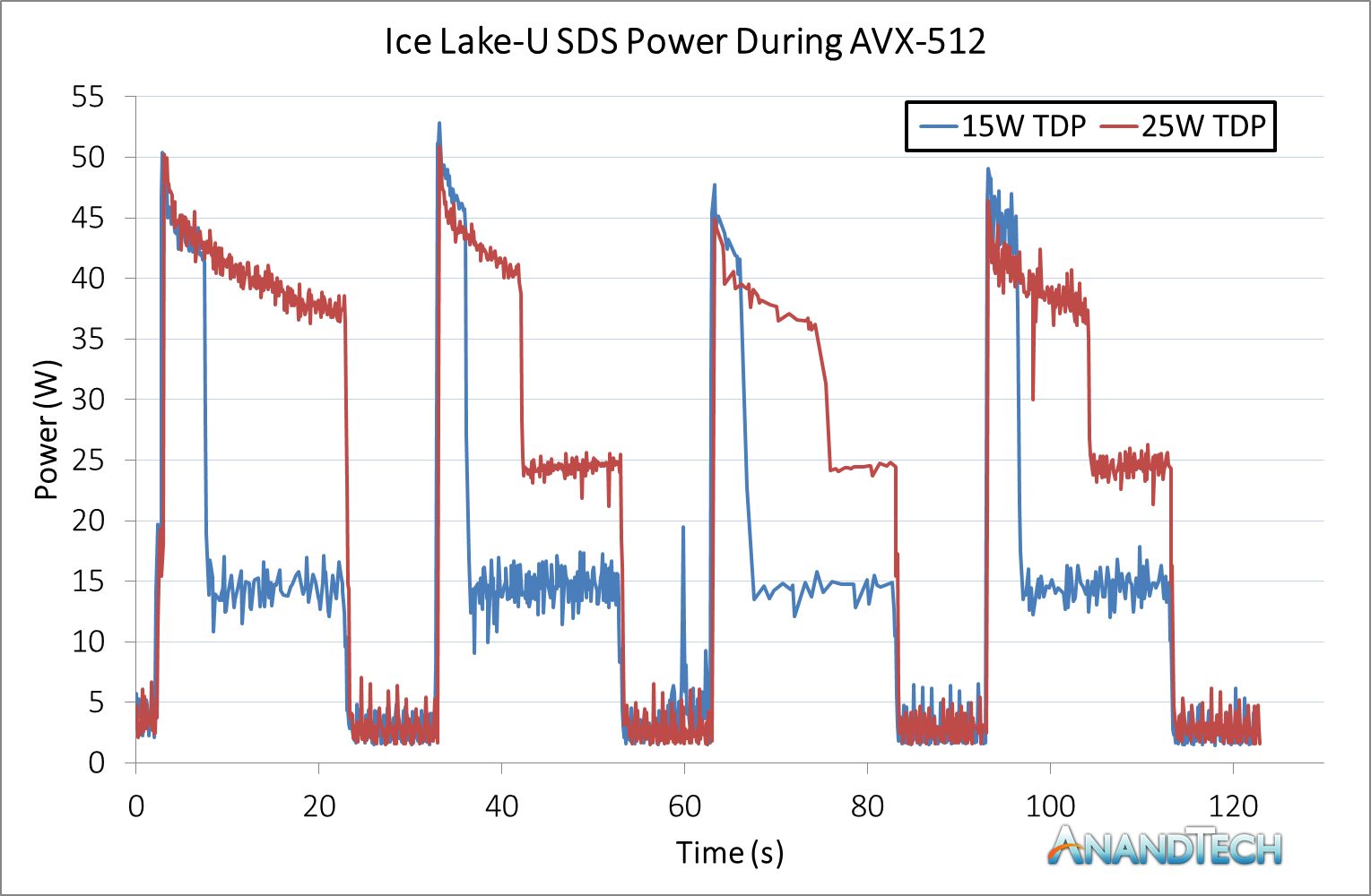
The test here runs for 20 seconds, then rests for 10 seconds. Here are the first four sub-tests, and there are a lot of interesting points to note.
The peak power in these systems is clearly the PL2 mode, which on the Intel SDS platform seems to be around the 50W mode. Given that the functional test system is a bit of a chonk, with a strong thermal profile and the fan on all the time, this is perhaps to be expected. The suggested PL2 for Kaby Lake-R was 44W, so this might indicate a small jump in strategy. Of course, with the Kaby Lake-R designs, we never saw many devices that actually had a PL2 of 44W – most OEMs chose something smaller, like 22W or 35W.
The fact that the CPU can sustain a 50W PL2 means that Intel could easily release Ice Lake into the desktop market at the 35W range. Easy. Please do this Intel.
Second to note is the AVX-512 frequency. Not listed here, but under the 15W mode we saw the AVX-512 frequency around 1.0-1.1 GHz, while at 25W it was around 1.4-1.5 GHz. That’s quite a drop from non AVX-512 code, for sure.
Third, we come to the turbo window. Increasing the base TDP means that the turbo window has more budget to turbo, and we can see that this equates to more than 2x on all the sub-tests. In the 15W mode, on the first test, we blow through the budget within 5 seconds, but on the 25W mode, we can actually turbo all the way through the 20 seconds of the first test. This means that there is still technically budget on the table by the time we start the second test under the 25W mode.
Also, that third test – if you are wondering why that graph looks a little light on the data points compared to the others, it is because the AVX-512 instructions took so much of the time on the CPU, that our power software didn’t get any for itself to update the power values. We still got enough to make a graph, but that just goes to show what hammering the CPU can do.
For the base power consumption, we actually have an issue here with the observer effect. Our polling software is polling too often and spiking up the power a little bit. However, if we take the average power consumption between 25-30 seconds, under 25W this is 2.96W, and under 15W this is 2.87W, which is similar.
For users interested in the score differential between the two:
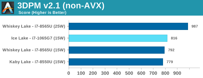
For 3DPM without AVX instructions, the 15W mode scored 816, and 25W mode scored 1020 (+25%).
For 3DPM with AVX-512, the 15W mode scored 7204, and 25W mode scored 9242 (+28%).
When testing a laptop system, there are various angles to consider on how to test: either user experience benchmarks, that are mostly single threaded and give a good boost to how systems implement a deal of turbo, or sustained benchmarks that test how the system performs when you push it. Intel has gone out of its way to emphasise the former for the next generation of mobile CPUs: they would prefer that reviewers stick to very user experience-like tests, rather than say, rendering programs. The problem there is that outside a number of canned benchmarks, it can be difficult. Users, and especially creators, that typically spend a lot on a premium device, might actually be doing sustained benchmarks.
Given the time that we had to test, we were actually limited in what we could arrange.
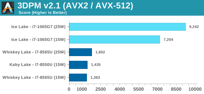
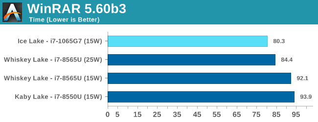
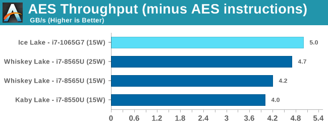
On AVX-512, the Ice Lake part destroys the competition.
These last two tests are typically our more memory sensitive tests, and the LPDDR4X-3733 really does win out over the LPDDR3-2133 in the other systems.
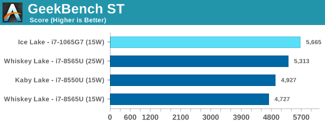
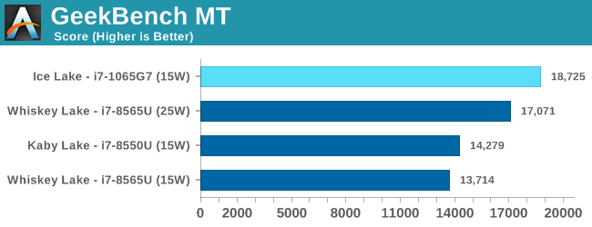
The realm of synthetic testing is a tricky one, given that there are plenty of benchmarks in the wild that provide a number, but aren’t actually based on real workloads, or are very limited in what they actually test. The issue here is that this software tries to emulate real-world, but it isn’t immersed in the harnesses or matrix of what a user might actually experience. For that reason, we only tend to use these benchmarks based on reader requests.
Legacy benchmarks are included for similar reasons, but can help to get a historical perspective.
One of the biggest changes to the Ice Lake design is in the integrated graphics – Intel is now giving more focus and more die area to graphics, something it has arguably been neglecting for several years now. With Ice Lake, we move to a Gen11 graphics architecture, which is almost like the previous Gen9.5 but now with added support for variable rate shading (VRS), moving from 24 EUs to 64 EUs, and memory support up from LPDDR3-2133 to LPDDR4X-3733.

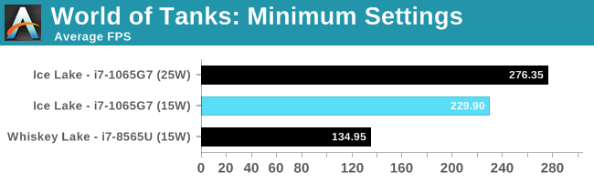
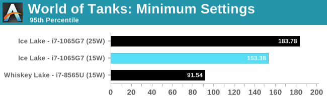
World of Tanks is a very CPU driven benchmark, and having the extra frequency of the 25W processor does help here. We're getting a sizeable uplift from Whiskey Lake, due to the extra EUs and memory frequency.

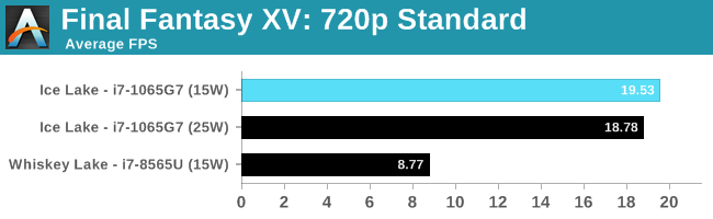
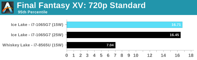
Our Final Fantasy test seemed to regress in 25W mode, although still within the noise. This test is still GPU bound, so adding the extra TDP to the CPU didn't actually help much. However, comparing to the Whiskey Lake integrated graphics, we've got over a 2x speedup.

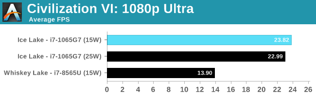
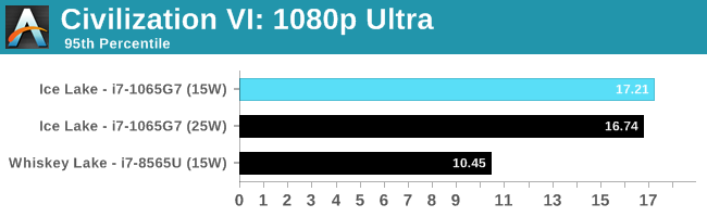
Similarly with Civilization, with what is normally our 'IGP' settings, we are still GPU limited here.
One of Intel's newest features is Variable Rate Shading.

If developers add the option, soon to be an easy checkbox in Unity and Unreal, the game can decide to control the rate at which it shades pixels, from calculating every pixel down using one result across a 4x4 grid, to save compute power. Currently the only way to test this is with the 3DMark functional demo.
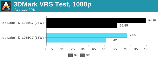
The new VRS test in 3DMark is designed as a feature test to show the potential uplift effect from enabling variable rate shading within a game. In both 15W and 25W modes, the data saw a good uplift, and we seemed to get more out of the 25W mode than the 15W mode.
First of all, I must say that Intel offering us to test a reference system in advance of a launch is a very good thing indeed. It is not something that Intel has done often in the past – in fact the last time I remember it happening was with Broadwell, when Intel sampled us one of their mobile CRB (consumer reference board) systems for the 45W chip. Before that, Intel had a small attempt allowing the press to benchmark Conroe in 2006 with canned pre-provided benchmarks, which did not go down to well. So moving into this pre-testing regime gets some immediate kudos to those who approved the testing.
Intel’s Broadwell / Crystalwell Mobile CRB
Given that the Ice Lake platform is more geared up towards ultra-premium designs, the software development system we ended up testing was certainly a reasonable expectation and direction that these parts would go in. Of course, we only had the best part of nine hours to test, and giving us the option to test both 15W and 25W modes meant we had to pick and choose what tests we thought were relevant. My most prominent feedback to Intel would be to give us two days to test next time, as it allows us to sit on our data after day one and decide what to do next. It was clear that some of the press in attendance only needed a day (or half a day), but for what we do at AT, then two days would be better.

The Intel Ice Lake SDS
As for Ice Lake itself, our results lean towards Ice Lake outperforming Whiskey Lake, if only by a small margin.
To preface this, I want to recall a graph that Intel showed off at Computex:
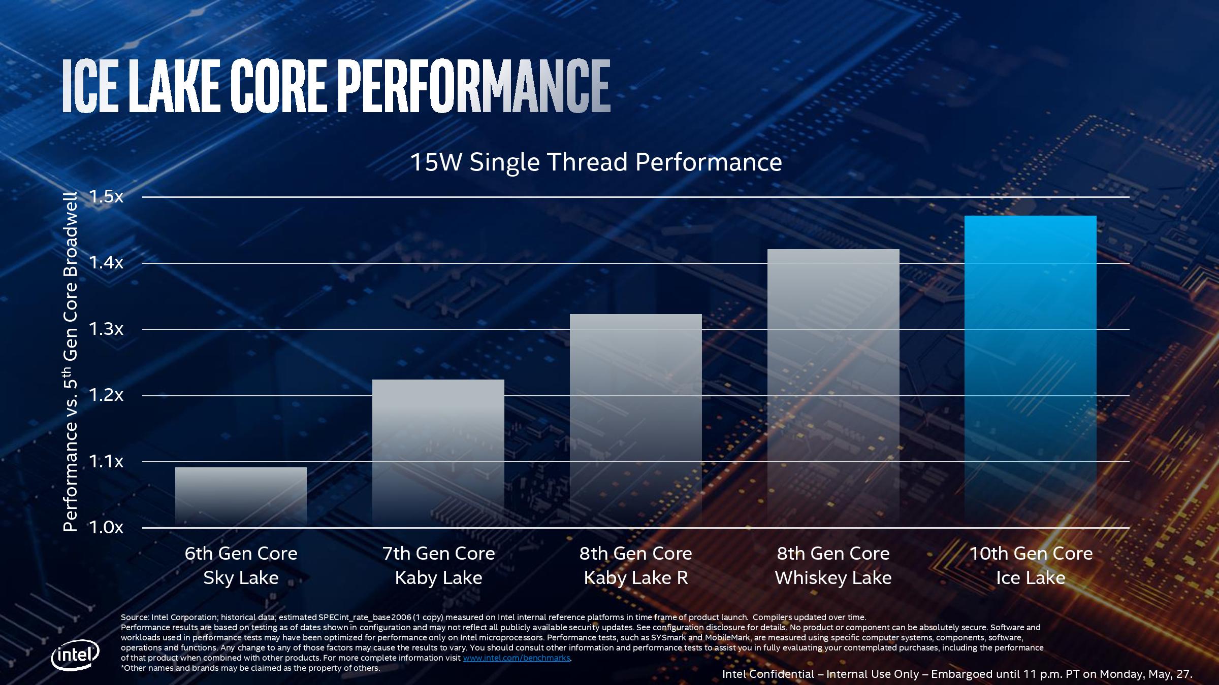
This graph shows the single thread performance of Skylake and beyond, compared to 5th Gen Broadwell hardware. Right at the very end, we see Whiskey Lake performing +42% above Broadwell, and Ice Lake performing +47% above Broadwell. A quick calculation of 1.47/1.42 means that even Intel is only predicting an absolute gain of ~3.5% for Ice Lake over current generation systems.
The reason why the difference is so small is because of IPC and frequency. Intel is touting a median IPC advantage on the new Sunny Cove cores of +18% against Skylake. That isn’t something we were able to test in the short time we had with the system, but +18% should provide a healthy bump – we actually see a number of key microarchitectural improvements bubble up through in our SPEC testing.
But at the same time, the frequency has decreased – our Whiskey Lake Huawei Matebook system was +500 MHz on the base frequency (+38%), and +700 MHz on the turbo frequency (+18%). If it were not for the vast increase in memory speed, moving from LPDDR3-2133 to LPDDR4X-3733, one might have predicted that the Core i7-1065G7 Ice Lake processor and the Core i7-8565U Whisky Lake processor would have performed equally.
The question here then becomes whether you prefer IPC or frequency. For instruction limited tasks, that answer should be IPC. For critical path limited tasks, you nominally require frequency. All this gets muddled a bit with the increased memory frequency, but with higher IPC at lower frequency, you should arguably be more power efficient as well, leading to longer battery life. At iso-performance between Ice and Whiskey, considering no other factors like price, I would choose Ice.
Intel has made a number of improvements to a chunk of the instruction set that should work well for users, however the new bigger cache design has added a bit of latency there, which ends up being a bit of give and take with cache hits and misses.
Of course, the one area where Ice Lake excels in is graphics. Moving from 24 EUs to 64 EUs, plus an increase in memory bandwidth to >50 GB/s, makes for some easy reading. It gets even better in 25W mode, for games that are CPU limited, but still don’t expect to be tackling AAA games at high resolutions. Despite Ice Lake being focused on the ultra-premium >1080p resolution market, you will still be gaming at 720p or 1080p at best here.
The other alternative is to attach a Thunderbolt 3 external graphics card. If there’s one really good add-in to Ice Lake, aside from the graphics uplift, it’s the inclusion of up to four TB3 ports as part of the CPU silicon. If and when the TB3 controllers get a lot cheaper on the device side, this should really help accelerate a high-performance standard here.
We should also talk about AVX-512 – Intel is in a position right now where including it in the chip uses a good amount of die area, and the software ecosystem hasn’t yet adopted it. By advertising speed-ups like DLBoost, the company is hoping to entice developers to work with AVX-512 in mind, and improve a number of machine learning applications for consumer processors. The other side there is what sort of consumer applications need machine learning that isn’t already done in the cloud. It’s a bit of a catch-22, but in our own testing, the AVX-512 does provide a significant speed-up. However, given Intel’s recent mantra of testing for user experience, it will be interesting to see how hammering the AVX-512 unit meshes with that mantra.
The scope of when these Ice Lake processors are coming to market, and how much, is still a question mark. Intel states that we’ll see Ice Lake in the market for the holiday season (i.e. Christmas), however we have a number of trade shows around the corner, such as IFA in September, where me might start seeing some companies start to show off their designs. We also know that Intel plans to release Comet Lake mobile processors sometime this year, on the old 14nm process and old Skylake-based microarchitecture, but at higher frequencies, so it will be interesting to see how they compete.
Final Thoughts
I’m glad to have tested Ice Lake. It’s a shame that we only had a day to test, because I could have spent a week testing that system. Increasing IPC is the best problem to solve, even if it gives similar performance due to a lower frequency, but hopefully the knock on effect here will be better battery life for users at the same performance. Once we get some systems in to test that battery life, and Project Athena’s requirement of 16+ hours comes to the front, I think we’ll see the best examples of Ice Lake shine through.
https://www.anandtech.com/show/14664/testing-intel-ice-lake-10nm
2019-08-01 13:31:03Z
52780343784745
Tidak ada komentar:
Posting Komentar