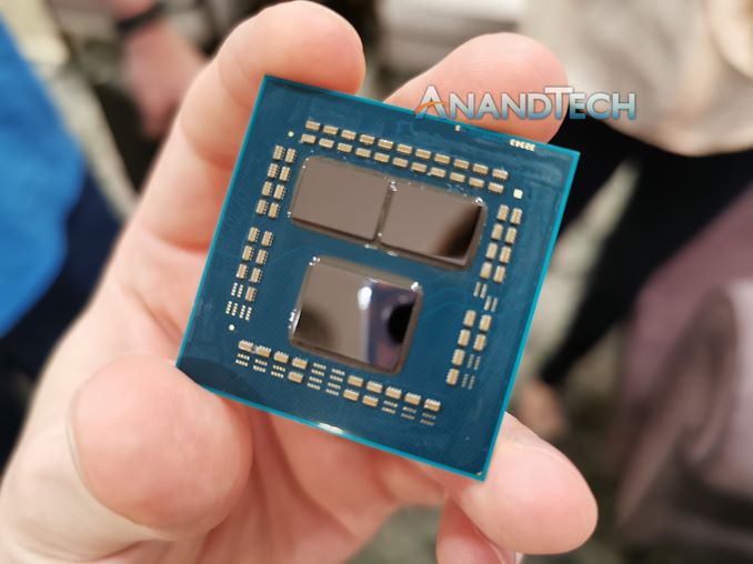
It’s the review we’ve all been waiting for. Since December last year – and particularly since CES – AMD has been teasing us about the new Zen 2 microarchitecture and AMD’s newest Ryzen 3000 series of CPUs. Incorporating a significantly upgraded CPU architecture and built using TSMC's latest generation manufacturing process, AMD has continued to run at full speed at a time when rival Intel has struggled to move at all. The end result is that while the first and second generation of Ryzen CPUs were all about AMD returning to competition and eating into Intel's substantial performance lead, the Ryzen 3000 series is nothing less than AMD's first shot in nearly 13 years at meeting (or beating) Intel at their own game in the desktop CPU market. It's a big moment for AMD, and an exciting one in the CPU industry as a whole.
The new Ryzen 3000 chips mark the first "big" leap for AMD since they introduced their first Ryzen processors a bit over two years ago. Unlike last year's Ryzen 2000 series, which was a more minor refresh and brought some tweaks to the microarchitecture and process node, this year’s Ryzen 3000 is a major upgrade for both CPU architecture as well as on the manufacturing node. It marks AMD’s switch from GlobalFoundries' 12nm process to TSMC’s newest 7nm node. But what’s more exciting is how AMD was able to actually implement this switch: Ryzen 3000 isn’t merely a single chip, but a collection of non-uniform chiplets, introducing this design paradigm in a consumer product for the first time.
Today AMD launches its entire new CPU lineup and platform, alongside the new Navi-based Radeon RX 5700 series. In terms of CPU coverage, we’ll be taking a closer look at the new flagship, the $499 12-core Ryzen 3900X, as well as the $329 8-core Ryzen 7 3700X and its peculiar low TDP of 65W.
The CPU Line-up
| AMD 'Matisse' Ryzen 3000 Series CPUs | |||||||||||
| AnandTech | Cores Threads |
Base Freq |
Boost Freq |
L2 Cache |
L3 Cache |
PCIe 4.0 |
Chiplets IO+CPU |
TDP | Price (SEP) |
||
| Ryzen 9 | 3950X | 16C | 32T | 3.5 | 4.7 | 8 MB | 64 MB | 16+4+4 | 1+2 | 105W | $749 |
| Ryzen 9 | 3900X | 12C | 24T | 3.8 | 4.6 | 6 MB | 64 MB | 16+4+4 | 1+2 | 105W | $499 |
| Ryzen 7 | 3800X | 8C | 16T | 3.9 | 4.5 | 4 MB | 32 MB | 16+4+4 | 1+1 | 105W | $399 |
| Ryzen 7 | 3700X | 8C | 16T | 3.6 | 4.4 | 4 MB | 32 MB | 16+4+4 | 1+1 | 65W | $329 |
| Ryzen 5 | 3600X | 6C | 12T | 3.8 | 4.4 | 3 MB | 32 MB | 16+4+4 | 1+1 | 95W | $249 |
| Ryzen 5 | 3600 | 6C | 12T | 3.6 | 4.2 | 3 MB | 32 MB | 16+4+4 | 1+1 | 65W | $199 |
AMD is launching 5 different SKUs today, with the 16-core Ryzen 9 3950X set to follow sometime in September. For today's launch AMD sampled the R9 3900X and R7 3700X, and we took them for a ride in the limited time we had with them, covering as much as we could.
Starting at the top we have the Ryzen 3900X, which is a 12-core design. In fact it's the first 12-core processor in a standard desktop socket, and it rather unique within AMD's product stack because it is currently the only SKU which takes full advantage of AMD’s newest chiplet architecture. Whereas all the other Ryzen parts are comprised of two chiplets – the base I/O die and a single CPU chiplet – 3900X comes with two such CPU chiplets, granting it (some of) the extra cores and the 64MB of L3 cache that entails.
Interestingly, while AMD has increased the core-count by 50% over its previous flagship processor, it has managed to keep the TDP to the same 105W as on the Ryzen 2700X. On top of this, the chip clocks in 300MHz faster than the predecessor in terms of boost clock, now reaching 4.6GHz; even the base clock has been increased by 100MHz, coming in at 3.8GHz. The big question then, is whether the new 7nm process node and Zen 2 are really this efficient, or should we be expecting more elevated power numbers?
Meanwhile our second chip of the day is the new Ryzen 3700X, which is configured and positioned as a particularly efficient model. With a boost clock of 4.4GHz and a base clock of 3.6GHz, the part should still be notably faster than the Ryzen 2700X, yet AMD has managed to make this a 65W TDP part which is going to make for some interesting analysis.
Continued Execution
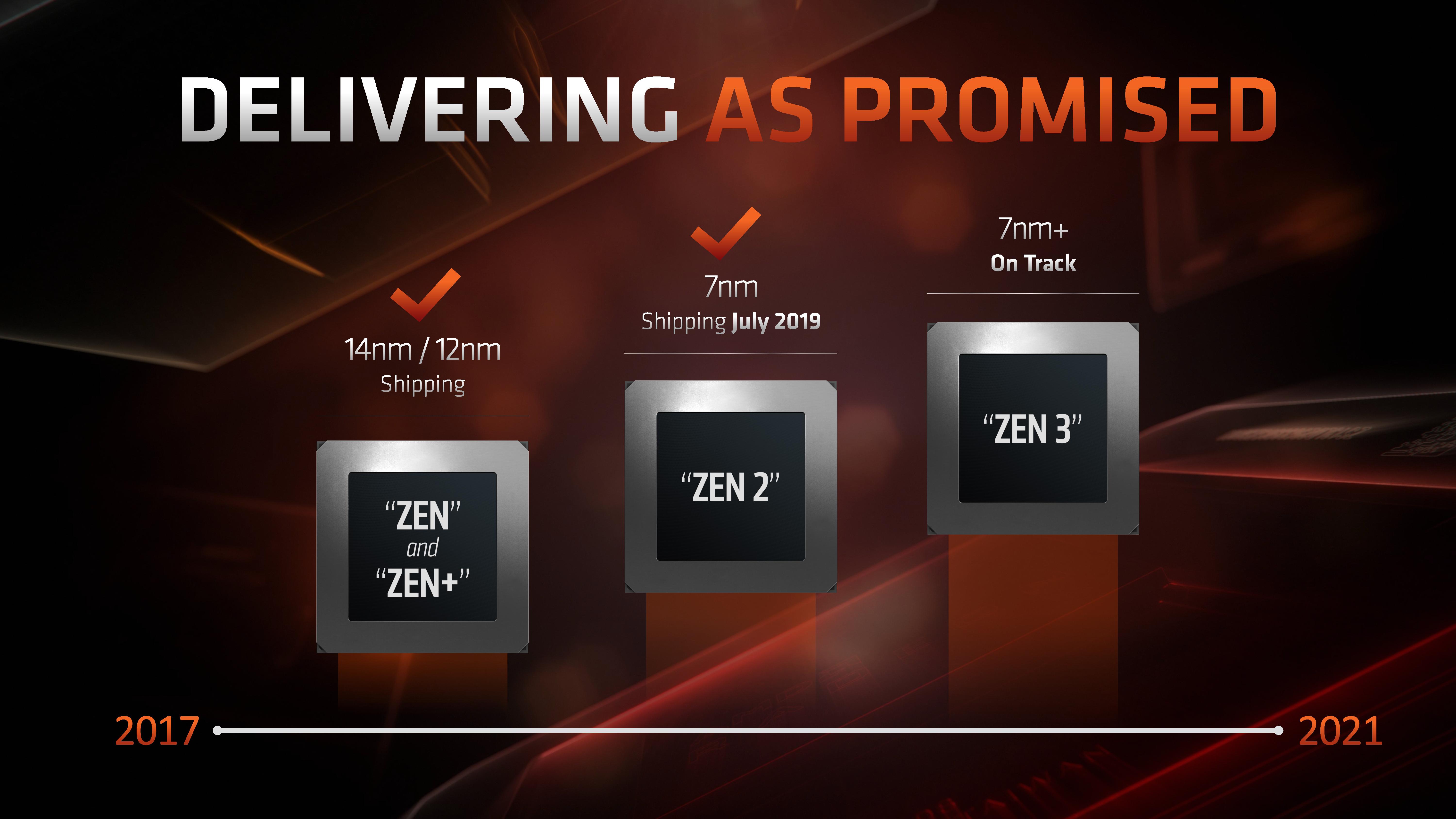
Today’s Zen 2 and Ryzen 3000 launch is another step forward on AMD’s roadmap. The company has been working on a very ambitious development roadmap for their CPU designs, and Zen 2 is the company's first chance to flex their muscles and do a full iteration on their CPU core design.
Executing on this roadmap has been important for AMD both because it's helped them close the performance gap with Intel, and because it's helped to prove to customers (particularly hyperscalers and enterprises) that Zen wasn't a fluke, and that the company can reliably continue to improve its technology. This is especially noteworthy because while rival Intel hasn't been standing still, all of Intel's desktop technology for the last 3 years has been based on the same Skylake core architecture and variations on Intel's exceptional-for-the-time 14nm process. This will eventually change, as Intel gets their desktop house in order for 2020, but right now AMD is moving forward when Intel can not, allowing AMD to take full advantage of Intel's run of bad luck and wooing customers in the process.
And of course, AMD isn't done here. For the company’s engineers, today’s chips are last year’s work, and the company is working on the next generation Zen 3 core. Zen 3 is still a full generation away – and today is all about Zen 2 – but AMD is making it clear that Zen 2 isn't the end of the road either, and that they are working to further improve their CPU microarchitecture and overall platform.
Large Performance Boosts, Particularly for Gaming
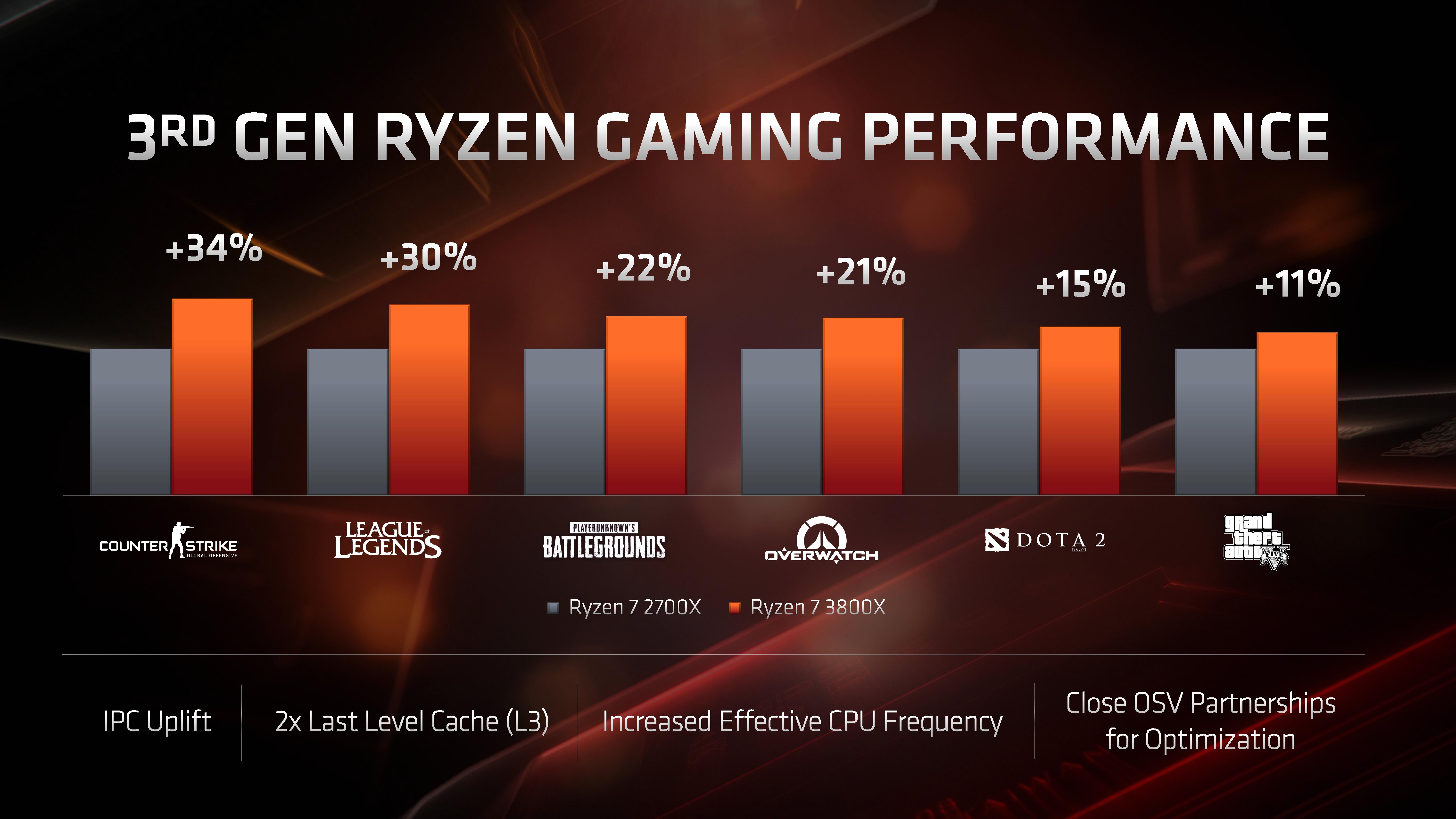
The 3rd gen Ryzen processors promise to bring some notably large performance improvements for users. The Zen 2 core microarchitecture is said to bring over 10% IPC improvements; this together with the higher clockspeeds should make for some solid generational improvements in a lot of workloads. For gaming in particular, AMD claims that we should be seeing some large improvements – the doubled size of the L3 cache is said to have made a notable mark on a lot of gaming titles, with AMD claiming ~20% to even ~30% improvements in some titles when compared to the last generation Ryzen 2700X.
Positioning the Ryzen 3000 series against Intel’s line-up is a matter of both performance as well as price. AMD had already made comparisons between the new SKUs and Intel’s counterparts back at Computex, where we saw comparisons between similarly priced units. According to the company, even Intel's pricey Skylake high-end desktop (HEDT) processor, the Core i9-9920X, isn't entirely out of the line of fire of the Ryzen 3900X.
As a quick recap to where things stand, compared to its immediate predecessor, Intel’s Coffee Lake Refresh received quite a bump in terms of both clock frequencies as well core counts. This allowed Intel to erase any Ryzen 2000 series lead in multi-threaded performance, all the while still maintaining a comfortable lead in single-threaded performance.
Against the Ryzen 3000 series, the Intel line-up will seemingly no longer have an IPC lead. AMD hasn’t been in such a situation since the Athlon 64 days well over 15 years ago, which is a remarkable turn of events. But with that said, make no mistake: IPC is just one half of the equation for single-threaded performance, and the other is raw frequency, and the Intel line-up still has a notable advantage thanks to its peak frequencies of up to 5GHz. So taking over Intel's single-threaded performance lead (at least on a consistent basis) is a tall order for the Ryzen 3000 series.
| Comparison: Ryzen 9 3900X vs Core i9-9900K | ||
| AMD Ryzen 9 3900X |
Features | Intel Core i9-9900K |
| 12 / 24 | Cores/Threads | 8 / 16 |
| 3.8 / 4.6 GHz | Base/Turbo | 3.6 / 5.0 GHz |
| 16 (Free) + 4 (NVMe) | PCIe 4.0 Lanes | 16 (Free) Gen 3.0 (No Gen 4.0) |
| 512 KB/core | L2 Cache | 256 KB/core |
| 4x 16 MB 64 MB total |
L3 Cache | 16 MB |
| 105 W | TDP | 95 W |
| $499 | Price (List) | $484 |
Taking a look at chip pricing and positioning then, the big flagship fight among desktop processors is going to be between the Ryzen 3900X at $484, and the i9-9900K at $484. Both of which happen to be the highest-end SKUs of their respective mainstream desktop computing platforms.
Here AMD should have a significant lead in terms of the multi-threaded performance of the new Ryzen 9 series as it’s able to employ 50% more cores than Intel, all while promising to remain in a similar TDP range of 105W vs 95W. We still expect the 9900K to win some workloads which are more lightly threaded simply due to Intel’s clock frequency lead, however this is something we’ll investigate more in detail in the coming benchmark analysis.
| Comparison: Ryzen 7 3700X vs Core i7-9700K | ||
| AMD Ryzen 7 3700X |
Features | Intel Core i7-9700K |
| 8 / 16 | Cores/Threads | 8 / 8 |
| 3.6 / 4.4 GHz | Base/Turbo | 3.6 / 4.9 GHz |
| 16 (Free) + 4 (NVMe) | PCIe 4.0 Lanes | 16 (Free) Gen 3.0 (No Gen 4.0) |
| 512 KB/core | L2 Cache | 256 KB/core |
| 2x 16 MB 32MB total |
L3 Cache | 12 MB |
| 65 W | TDP | 95 W |
| $329 | Price (List) | $385 |
The Ryzen 7 3700X is an interesting SKU. With only one populated CPU chiplet, the unit has half the available L3 cache versus the Ryzen 9 3900X. But it also has all the CPU cores within its one chiplet active. In theory this does mean that the CPU cores have less overall L3 cache available to them, as they have to share it with an additional core within their respective CCXs.
With a 3.6GHz/4.4Ghz base/boost clock configuration, we expect the 3700X to outperform the previous generation 2700X in all scenarios. The competition here based on pricing is the Core i7-9700K. Intel again should have a single-threaded performance advantage thanks to its 500 MHz higher clocks – but we’ll have to see how both chips match up in daily workloads.
We’ve already posted a microarchitecture overview and analysis of the Zen 2 microarchitecture following our Tech Day briefings in June, so be sure to read the piece in preparation for further testing analysis in our review today:
Read: AMD Zen 2 Microarchitecture Analysis: Ryzen 3000 and EPYC Rome
Among the biggest changes of the Ryzen 3000, alongside the improved core microarchitecture, is the chip’s overall cache hierarchy. The new chiplet houses CCXes with double the amount of L3, now 16MB instead of 8MB.
Furthermore the chiplet design with the introduction of the cIO die which houses the new memory controllers are undoubtedly going to have an impact on the memory latency and performance of the overall chip.
On the memory controller side particularly, AMD promises a wholly revamped design that brings new support for a whole lot faster DDR4 modules, with the chip coming by default categorized as supporting DDR4-3200, which is a bump over the DDR-2933 support of the Ryzen 2000 series.
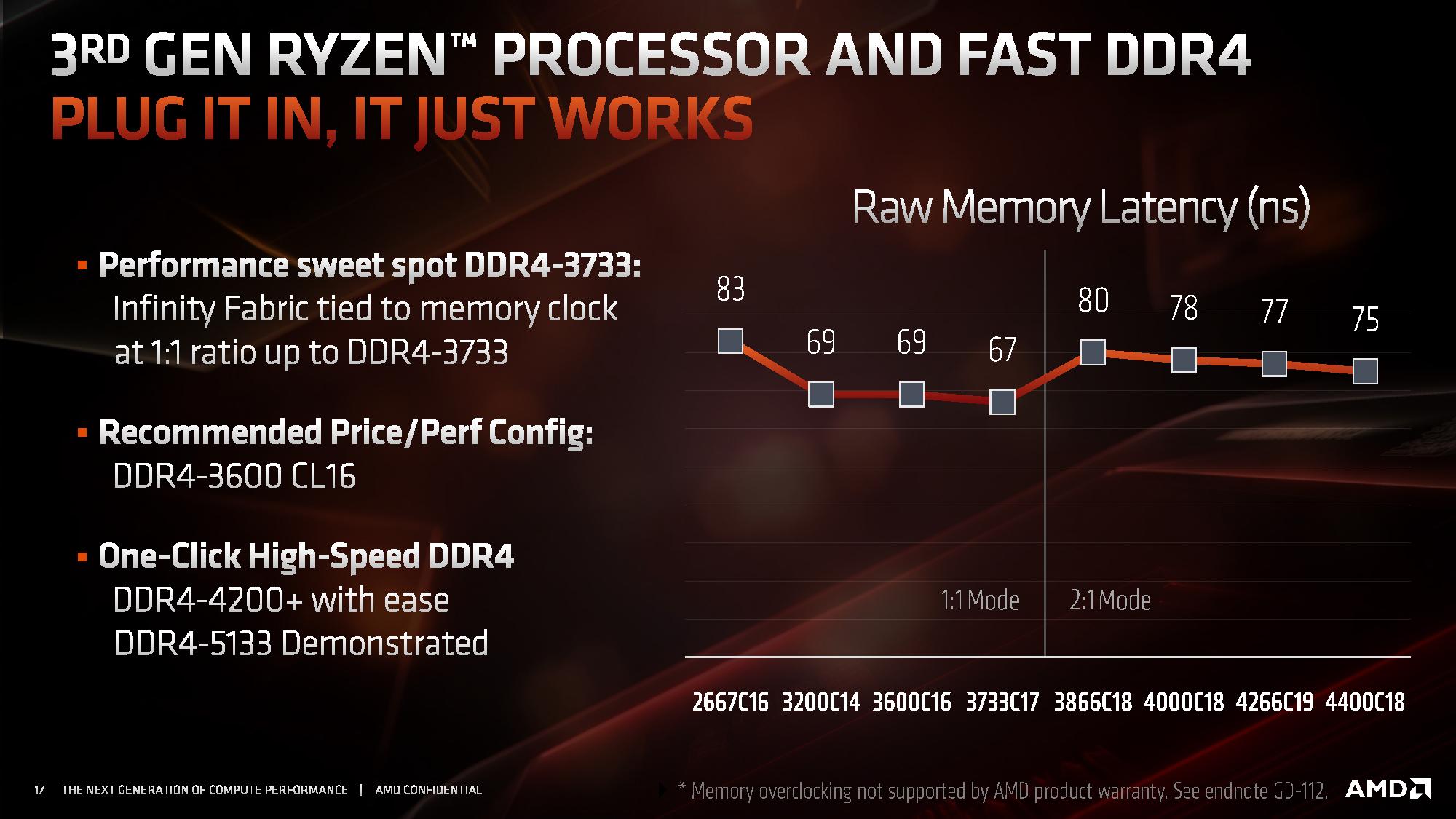
AMD had published an interesting slide in regards to the new faster DDR support that went well above the officially supported 3200 speeds, with AMD claiming that the new controllers are able to support up to DDR4-4200 with ease and overclocking being possible to achieve ever higher speeds. However there’s a catch: in order to support DDR4 above 3600, the chip will automatically change the memory controller to infinity fabric clock ratio from being 1:1 to 2:1.
Whilst this doesn’t bottleneck the bandwidth of the memory to the cores as the new microarchitecture has now doubled the bus width of the Infinity Fabric to 512 bits, it does add a notable amount of cycles to the overall memory latency, meaning for the very vast majority of workloads, you’re better off staying at or under DDR4-3600 with a 1:1 MC:IF ratio. It’s to be noted that it’s still possible to maintain this 1:1 ratio by manually adjusting it at higher MC speeds, however stability of the system is no longer guaranteed as you’re effectively overclocking the Infinity Fabric as well in such a scenario.
For this article we didn’t have enough time to dive into the scaling behaviour of the different DRAM speeds, what we did investigate is a more architectural question of how exactly the new chiplet and cIO die architecture has impacted Zen2’s memory latency and memory performance.
To give better insights, we’re using my custom memory latency test that I use for mobile SoC testing and first covered in our review of the Galaxy S10+ and its two SoCs. Memory latency testing nowadays is a complicated topic as microarchitectures advance at a rapid rate, and in particular prefetchers can cause for sometimes misleading figures. Similarly, more brute-force approaches such as full random tests contain a lot of TLB miss latencies which don’t represent the actual structural latency of the system. Our custom latency suite thus isn’t a single one-number-fits-all test but rather a collection of tests that expose more details of the memory behaviour of the system.
The figures published on this page are run on DDR4-3200CL16 on the Ryzen 3900X and 2700X at timings of 16-16-16-36, and the i9-9900K was run with similar DDR4-3200CL16 at timings of 16-18-18-36.
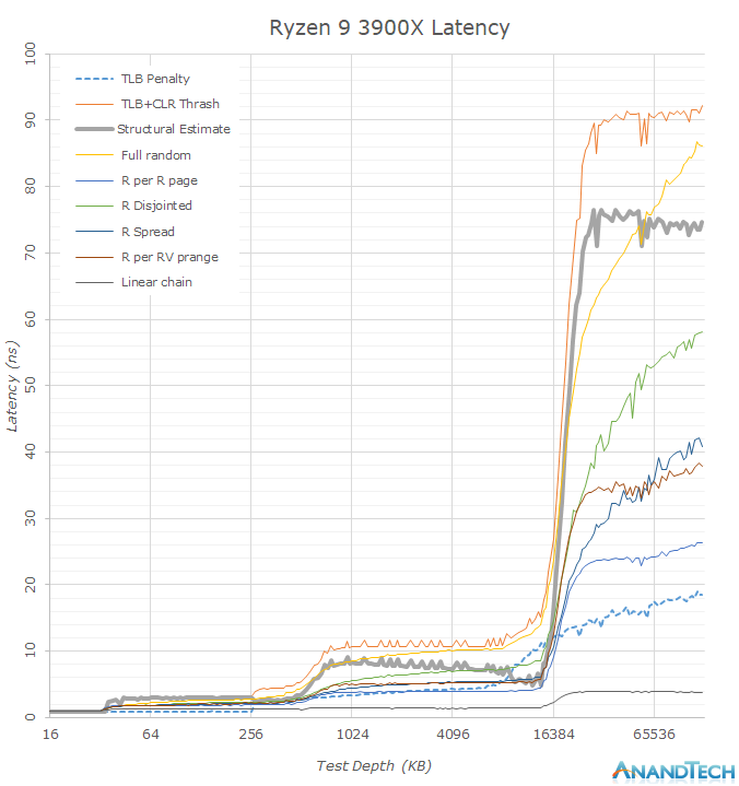
Looking at the memory latency curves in a linear plotted graph, we see that there’s some larger obvious differences between the new Ryzen 3900X and the Ryzen 2700X. What immediately catches the eye when switching between the two results is the new 16MB L3 cache capacity which doubles upon the 8MB of Matisse. We have to remind ourselves that even though the whole chip contains 64MB of L3 cache, this is not a unified cache and a single CPU core will only see its own CCX’s L3 cache before going into main memory, which is in contrast to Intel’s L3 cache where all the cores have access to the full amount.
Before going into more details in the next graph, another thing that is obvious is that seemingly the 3900X’s DRAM latency is a tad worse than the 2700X’s. Among the many test patterns here the one to note is the “Structural Estimate” curve. This curve is actually a simple subtraction of the TLB+CLR Thrash tests minus the TLB Penalty figure. In the former, we’re causing as much cache-line replacement pressure as possible by repeatedly hitting the same cacheline within each memory page, also repeatedly trying to miss the TLB. In the latter, we’re still hitting the TLB heavily, but always using a different cache-line and thus having a minimum of cache-line pressure, resulting in an estimate of the TLB penalty. Subtracting the latter from the former gives us a quite good estimate of the actual structural latency of the chip and memory.
Now the big question is, why do it this way? I’ve found that with increasingly better prefetchers, it’s getting difficult in getting good memory latency numbers. Whilst it’s possible to just outright disable prefetchers on some platforms, that avenue isn’t always available.
Precisely when looking at the other various patterns in the graph, we’re seeing quite a large difference between the 3900X and the 2700X, with the 3900X showcasing notably lower latencies in a few of them. These figures are now a result of the new Zen2’s improved prefetchers which are able to better recognize patterns and pull out data from DRAM before the CPU core will handle that memory address.
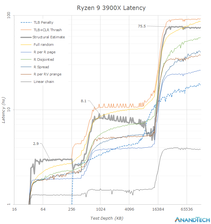
Plotting the same data on a logarithmic graph, we better see some of the details.
In terms of the DRAM latency, it seems that the new Ryzen 3900X has regressed by around 10ns when compared to the 2700X (Note: Just take into the leading edge of the “Structural Estimate” figures as the better estimate) with ~74-75.5ns versus ~65.7ns.
It also looks like Zen2’s L3 cache has also gained a few cycles: A change from ~7.5ns at 4.3GHz to ~8.1ns at 4.6GHz would mean a regression from ~32 cycles to ~37 cycles. Such as change however was to be expected since doubling of the L3 cache structure has to come with some implementation compromises as there’s never just a free lunch. Zen2’s L3 cache latency is thus now about the same as Intel’s – while it was previously faster on Zen+.
Further interesting characteristics we see here is the increase of the capacity of the L2 TLB. This can be seen in the “TLB Penalty” curve, and the depth here corresponds to AMD’s published details of increasing the structure from 1536 pages to 2048 pages. It’s to be noted that the L3 capacity now exceeds the capacity of the TLB, meaning a single CPU core will have only the best access latencies to up to 8MB in the cache before starting to have to page-walk. A similar behaviour we see in the L2 cache where the L1 TLB capacity only covers 256KB of the cache before having to look up entries in the L2 TLB.
Another very interesting characteristic of AMD’s microarchitecture which contrasts Intel’s, is the fact that AMD prefetchers into the L2 cache, while Intel only does so for the nearest cache-line. Such a behaviour is a double-edged sword, on one hand AMD’s cores have can have better latencies to needed data, but on the other hand in the case of a unneeded prefetch, this put a lot more pressure on the L2 cache capacity, and could in effect counter-act some of the benefits of having double the capacity over Intel’s design.
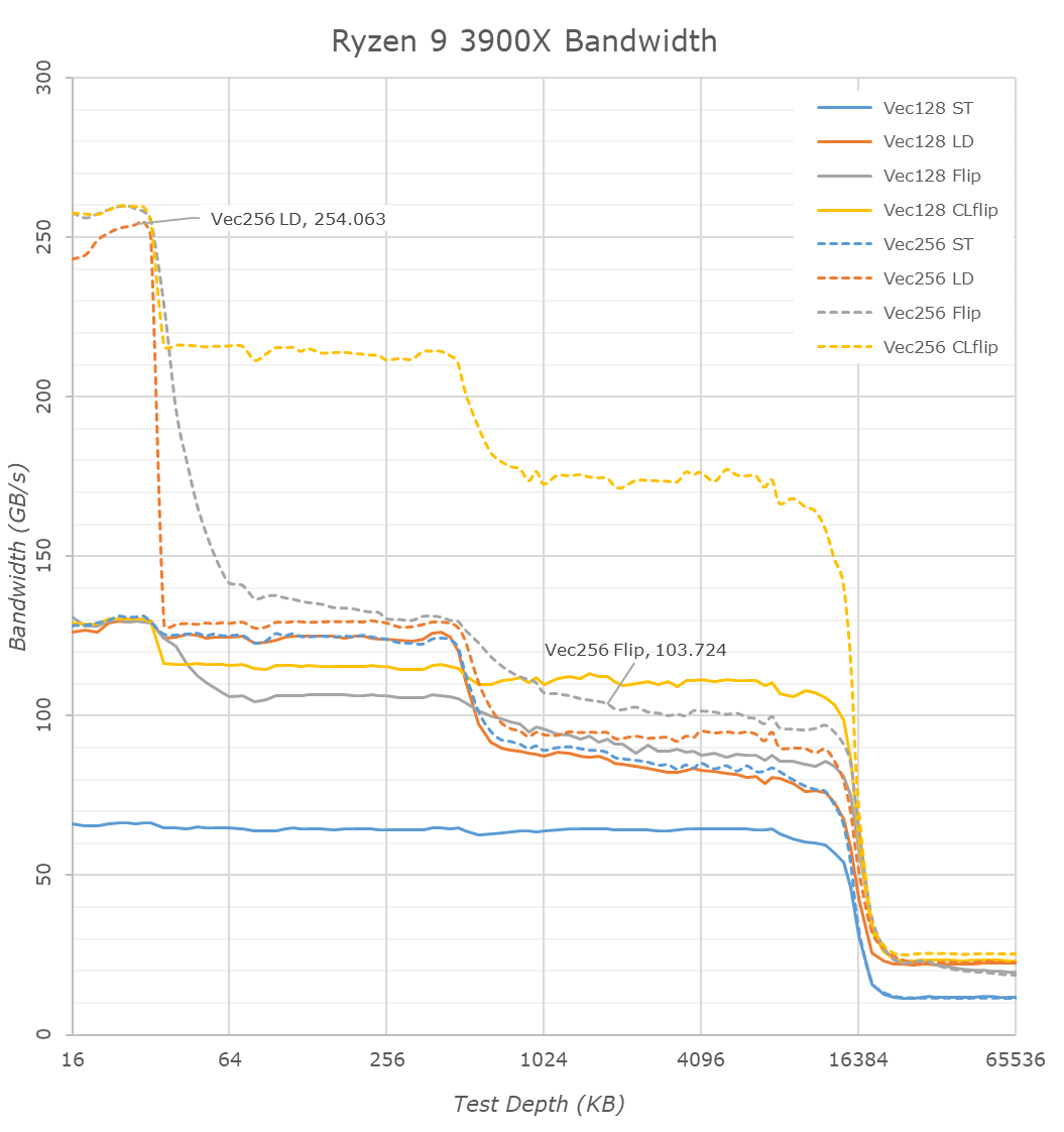
Switching over to the memory bandwidth of the cache hierarchy, there’s one obvious new chance in the 3900X and Zen2: the inclusion of 256-bit wide datapaths. The new AGU and path changes mean that the core is able to now handle 256-bit AVX instruction once per cycle which is a doubling over the 128-bit datapaths of Zen and Zen+.
So while the bandwidth of 256-bit operations on the Ryzen 2700X looked identical to the 128-bit variants, the wider ops now on Zen2 effectively double the bandwidth of the core. This bandwidth doubling is evident in the L1 cache (The flip test is equal to a memory copy test), however the increase is only about 20% for the L2 and L3 caches.
There’s an interesting juxtaposition between AMD’s L3 cache bandwidth and Intel’s: AMD here has essentially as 60% advantage in bandwidth as the CCX’s L3 is much faster than Intel’s L3, when accessed by a single core. Particularly read-write modifications within a single cache-line (CLflip test) are significantly faster in both the L2 and L3 caches when compared to Intel’s core design.
Deeper into the DRAM regions, however we see that AMD is still lagging behind Intel when it comes to memory controller efficiency, so while the 3900X improves copy bandwidth from 19.2GB/s to 21GB/s, it still remains behind the 9900K’s 22.9GB/s. The store bandwidth (write bandwidth) to memory is also a tad lower on the AMD parts as the 3900X reaches 14.5GB/s versus Intel’s 18GB/s.
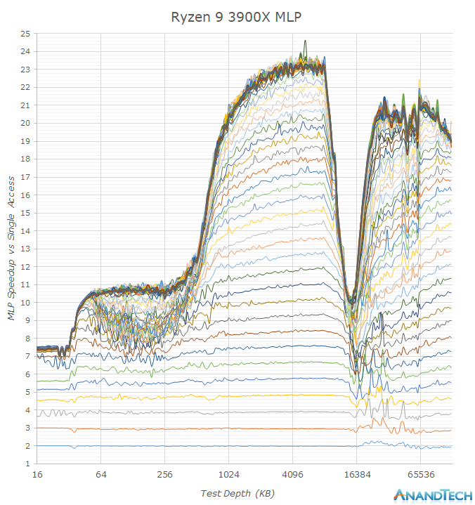
One aspect that AMD excels in is memory level parallelism. MLP is the ability for the CPU core to “park” memory accesses when they are missing the caches, and wait on them to return back later. In the above graph we see increasing number of random memory accesses depicted as the stacked lines, with the vertical axis showcasing the effective access speedup in relation to a single access.
Whilst both AMD and Intel’s MLP ability in the L2 are somewhat the same and reach 12 – this is because we’re saturating the bandwidth of the cache in this region and we just can’t go any faster via more accesses. In the L3 region however we see big differences between the two: While Intel starts off with around 20 accesses at the L3 with a 14-15x speedup, the TLBs and supporting core structures aren’t able to sustain this properly over the whole L3 as it’s having to access other L3 slices on the chip.
AMD’s implementation however seems to be able to handle over 32 accesses with an extremely robust 23x speedup. This advantage actually continues on to the DRAM region where we still see speed-ups up to 32 accesses, while Intel peaks at 16.
MLP ability is extremely important in order to be able to actually hide the various memory hierarchy latencies and to take full advantage of a CPU’s out-of-order execution abilities. AMD’s Zen cores here have seemingly the best microarchitecture in this regard, with only Apple’s mobile CPU cores having comparable characteristics. I think this was very much a conscious design choice of the microarchitecture as AMD knew their overall SoC design and future chiplet architecture would have to deal with higher latencies, and did their best in order to minimise such a disadvantage.
So while the new Zen2 cores do seemingly have worse off latencies, possibly a combined factor of a faster memory controller (faster frequencies could have come at a cost of latency in the implementation), a larger L3 but with additional cycles, it doesn’t mean that memory sensitive workloads will see much of a regression. AMD has been able to improve the core’s prefetchers, and average workload latency will be lower due to the doubled L3, and this is on top the core’s microarchitecture which seems to have outstandingly good MLP ability for whenever there is a cache miss, something to keep in mind as we investigate performance further.
Section by Gavin Bonshor
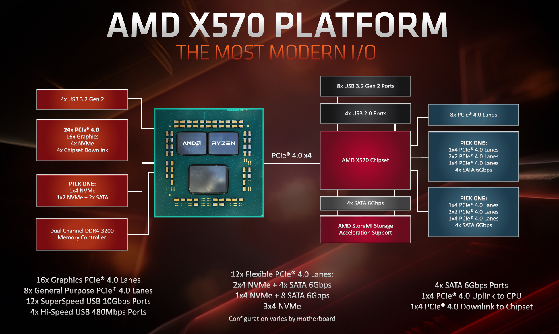
One of the biggest additions to AMD's AM4 socket is the introduction of the PCIe 4.0 interface. The new generation of X570 motherboards marks the first consumer motherboard chipset to feature PCIe 4.0 natively, which looks to offer users looking for even faster storage, and potentially better bandwidth for next-generation graphics cards over previous iterations of the current GPU architecture. We know that the Zen 2 processors have implemented the new TSMC 7nm manufacturing process with double the L3 cache compared with Zen 1. This new centrally focused IO chiplet is there regardless of the core count and uses the Infinity Fabric interconnect; the AMD X570 chipset uses four PCIe 4.0 lanes to uplink and downlink to the CPU IO die.
Looking at a direct comparison between AMD's AM4 X series chipsets, the X570 chipset adds PCIe 4.0 lanes over the previous X470 and X370's reliance on PCIe 3.0. A big plus point to the new X570 chipset is more support for USB 3.1 Gen2 with AMD allowing motherboard manufacturers to play with 12 flexible PCIe 4.0 lanes and implement features how they wish. This includes 8 x PCIe 4.0 lanes, with two blocks of PCIe 4.0 x4 to play with which vendors can add SATA, PCIe 4.0 x1 slots, and even support for 3 x PCIe 4.0 NVMe M.2 slots.
| AMD X570, X470 and X370 Chipset Comparison | |||
| Feature | X570 | X470 | X370 |
| PCIe Interface | 4.0 | 3.0 | 3.0 |
| Max PCH PCIe Lanes | 24 | 24 | 24 |
| USB 3.1 Gen2 | 8 | 2 | 2 |
| Max USB 3.1 (Gen2/Gen1) | 8/4 | 2/6 | 2/6 |
| DDR4 Support | 3200 | 2933 | 2667 |
| Max SATA Ports | 8 | 8 | 8 |
| PCIe GPU Config | x16 x8/x8 x8/x8/x8* |
x16 x8/x8 x8/x8/x4 |
x16 x8/x8 x8/x8/x4 |
| Memory Channels (Dual) | 2/2 | 2/2 | 2/2 |
| Integrated 802.11ac WiFi MAC | N | N | N |
| Chipset TDP | 15/11W** | 6.8W | 4.8W |
| Overclocking Support | Y | Y | Y |
| XFR2/PB2 Support | Y | Y | N |
* Due to two different variations of the X570 chipset, one with a 15 W and another with an 11 W TDP, the extra power allows for more PCIe lanes, thus better GPU support overall. One example is the ASUS Pro WS X570-Ace model.
** Same reason as above, adding extra PCIe lanes to the chipset naturally increases power consumption.
One of the biggest changes in the chipset is within its architecture. The X570 chipset is the first chipset its manufactured in-house using ASMedia's IP, whereas previously with the X470 and X370 chipsets, ASMedia developed and produced it based on its 55nm architecture. While going from X370 at 6.8 W TDP at maximum load, X470 was improved upon in terms of power consumption to a lower TDP of 4.8 W. For X570, this has increased massively to an 11 W TDP on its consumer models, with a 15 W variant for its more professional and enterprise-focused models. The difference between the two X570 variations aside from power consumption is that the 15 W X570 chipset adds extra PCIe 4.0 lanes which seemingly increases power consumption greatly when compared to previous PCIe 3.0 focused chipsets.
Another major change due to the increased power consumption of the X570 chipset when compared to X470 and X370 is the cooling required. All but one of the launched product stack features an actively cooled chipset heatsink which is needed due to the increased power draw when using PCIe 4.0 due to the more complex implementation requirements over PCIe 3.0. While it is expected AMD will work on improving the TDP on future generations when using PCIe 4.0, it's forced manufacturers to implement more premium and more effective ways of keeping componentry on X570 cooler. This also stretches to the power delivery as AMD announced that a 16-core desktop Ryzen 3950X processor is set to launch later on in the year which means motherboard manufacturers need to implement better power deliveries, and better heatsinks capable of keeping the 105 W TDP processors efficient.
Memory support has also been improved with a seemingly better IMC on the Ryzen 3000 line-up when compared against the Ryzen 2000 and 1000 series of processors. Some motherboard vendors are advertising speeds of up to DDR4-4400 which until X570, was unheard of. X570 also marks a jump up to DDR4-3200 up from DDR4-2933 on X470, and DDR4-2667 on X370. As we investigated in our Ryzen 7 Memory Scaling piece back in 2017, we found out that the Infinity Fabric Interconnect scales well with frequency, and it is something that we will be analyzing once we get the launch of X570 out of the way, and potentially allow motherboard vendors to work on their infant firmware for AMD's new 7nm silicon.
Section by Dr. Ian Cutress (Orignal article)
One of the key points that have been a pain in the side of non-Intel processors using Windows has been the optimizations and scheduler arrangements in the operating system. We’ve seen in the past how Windows has not been kind to non-Intel microarchitecture layouts, such as AMD’s previous module design in Bulldozer, the Qualcomm hybrid CPU strategy with Windows on Snapdragon, and more recently with multi-die arrangements on Threadripper that introduce different memory latency domains into consumer computing.
Obviously AMD has a close relationship with Microsoft when it comes down to identifying a non-regular core topology with a processor, and the two companies work towards ensuring that thread and memory assignments, absent of program driven direction, attempt to make the most out of the system. With the May 10th update to Windows, some additional features have been put in place to get the most out of the upcoming Zen 2 microarchitecture and Ryzen 3000 silicon layouts.
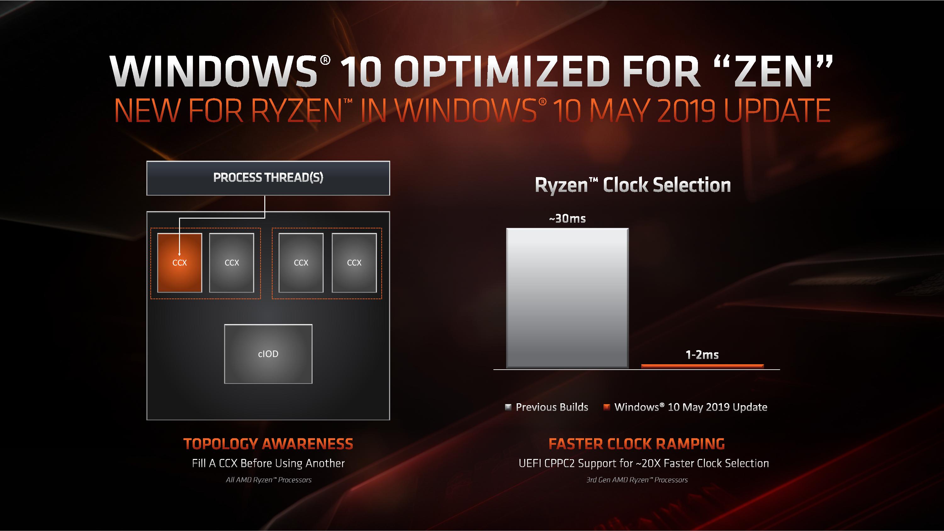
The optimizations come on two fronts, both of which are reasonably easy to explain.
Thread Grouping
The first is thread allocation. When a processor has different ‘groups’ of CPU cores, there are different ways in which threads are allocated, all of which have pros and cons. The two extremes for thread allocation come down to thread grouping and thread expansion.
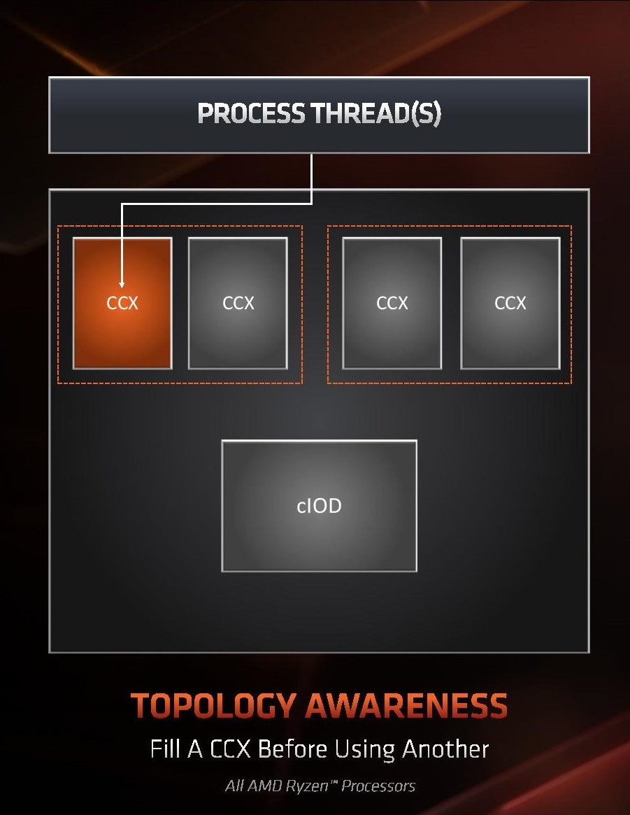
Thread grouping is where as new threads are spawned, they will be allocated onto cores directly next to cores that already have threads. This keeps the threads close together, for thread-to-thread communication, however it can create regions of high power density, especially when there are many cores on the processor but only a couple are active.
Thread expansion is where cores are placed as far away from each other as possible. In AMD’s case, this would mean a second thread spawning on a different chiplet, or a different core complex/CCX, as far away as possible. This allows the CPU to maintain high performance by not having regions of high power density, typically providing the best turbo performance across multiple threads.
The danger of thread expansion is when a program spawns two threads that end up on different sides of the CPU. In Threadripper, this could even mean that the second thread was on a part of the CPU that had a long memory latency, causing an imbalance in the potential performance between the two threads, even though the cores those threads were on would have been at the higher turbo frequency.
Because of how modern software, and in particular video games, are now spawning multiple threads rather than relying on a single thread, and those threads need to talk to each other, AMD is moving from a hybrid thread expansion technique to a thread grouping technique. This means that one CCX will fill up with threads before another CCX is even accessed. AMD believes that despite the potential for high power density within a chiplet, while the other might be inactive, is still worth it for overall performance.
For Matisse, this should afford a nice improvement for limited thread scenarios, and on the face of the technology, gaming. It will be interesting to see how much of an affect this has on the upcoming EPYC Rome CPUs or future Threadripper designs. The single benchmark AMD provided in its explanation was Rocket League at 1080p Low, which reported a +15% frame rate gain.
Clock Ramping
For any of our users familiar with our Skylake microarchitecture deep dive, you may remember that Intel introduced a new feature called Speed Shift that enabled the processor to adjust between different P-states more freely, as well as ramping from idle to load very quickly – from 100 ms to 40ms in the first version in Skylake, then down to 15 ms with Kaby Lake. It did this by handing P-state control back from the OS to the processor, which reacted based on instruction throughput and request. With Zen 2, AMD is now enabling the same feature.

AMD already has sufficiently more granularity in its frequency adjustments over Intel, allowing for 25 MHz differences rather than 100 MHz differences, however enabling a faster ramp-to-load frequency jump is going to help AMD when it comes to very burst-driven workloads, such as WebXPRT (Intel’s favorite for this sort of demonstration). According to AMD, the way that this has been implemented with Zen 2 will require BIOS updates as well as moving to the Windows May 10th update, but it will reduce frequency ramping from ~30 milliseconds on Zen to ~1-2 milliseconds on Zen 2. It should be noted that this is much faster than the numbers Intel tends to provide.
The technical name for AMD’s implementation involves CPPC2, or Collaborative Power Performance Control 2, and AMD’s metrics state that this can increase burst workloads and also application loading. AMD cites a +6% performance gain in application launch times using PCMark10’s app launch sub-test.
Hardened Security for Zen 2
Another aspect to Zen 2 is AMD’s approach to heightened security requirements of modern processors. As has been reported, a good number of the recent array of side channel exploits do not affect AMD processors, primarily because of how AMD manages its TLB buffers that have always required additional security checks before most of this became an issue. Nonetheless, for the issues to which AMD is vulnerable, it has implemented a full hardware-based security platform for them.
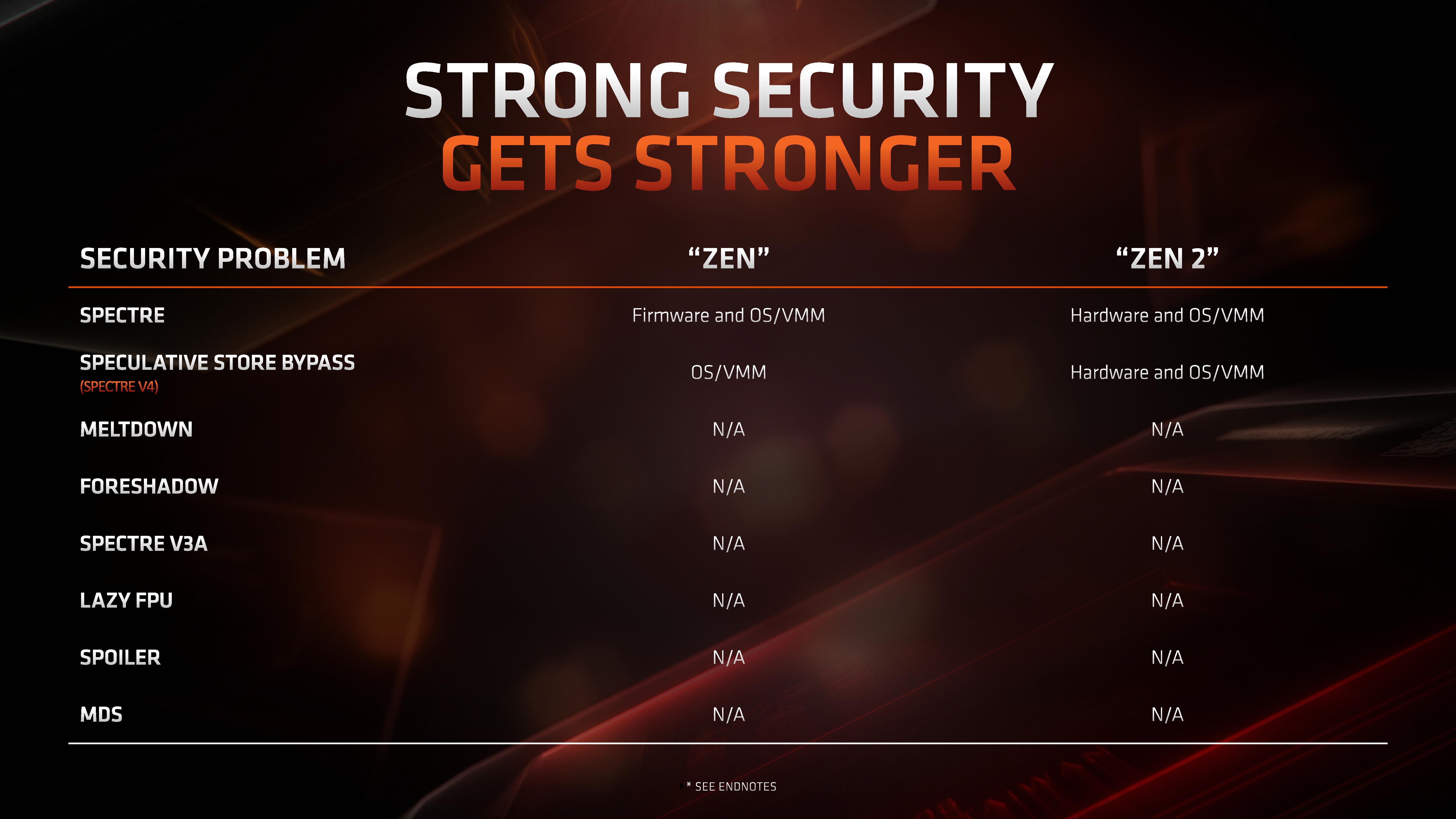
The change here comes for the Speculative Store Bypass, known as Spectre v4, which AMD now has additional hardware to work in conjunction with the OS or virtual memory managers such as hypervisors in order to control. AMD doesn’t expect any performance change from these updates. Newer issues such as Foreshadow and Zombieload do not affect AMD processors.
One big talking point around the new Ryzen 3000 series is the new augmented single-threaded performance of the new Zen 2 core. In order to investigate the topic in a more controlled manner with better documented workloads, we’ve fallen back to the industry standard SPEC benchmark suite.
We’ll be investigating the previous generation SPEC CPU2006 test suite giving us some better context to past platforms, as well as introducing the new SPEC CPU2017 suite. We have to note that SPEC2006 has been deprecated in favour of 2017, and we must also mention that the scores posted today are noted as estimates as they’re not officially submitted to the SPEC organisation.
For SPEC2006, we’re still using the same setup as on our mobile suite, meaning all the C/C++ benchmarks, while for SPEC2017 I’ve also went ahead and prepared all the Fortran tests for a near complete suite for desktop systems. I say near complete as due to time constraints we’re running the suite via WSL on Windows. I’ve checked that there are no noticeable performance differences to native Linux (we’re also compiling statically), however one bug on WSL is that it has a fixed stack size so we’ll be missing 521.wrf_r from the SPECfp2017 collection.
In terms of compilers, I’ve opted to use LLVM both for C/C++ and Fortran tests. For Fortran, we’re using the Flang compiler. The rationale of using LLVM over GCC is better cross-platform comparisons to platforms that have only have LLVM support and future articles where we’ll investigate this aspect more. We’re not considering closed-sourced compilers such as MSVC or ICC.
clang version 8.0.0-svn350067-1~exp1+0~20181226174230.701~1.gbp6019f2 (trunk)
clang version 7.0.1 (ssh://git@github.com/flang-compiler/flang-driver.git
  24bd54da5c41af04838bbe7b68f830840d47fc03)

-Ofast -fomit-frame-pointer
-march=x86-64
-mtune=core-avx2
-mfma -mavx -mavx2
Our compiler flags are straightforward, with basic –Ofast and relevant running and ISA switches to allow for AVX2 instructions.
The Ryzen 3900X system was run in the same way as the rest of our article with DDR4-3200CL16, same as with the i9-9900K, whilst the Ryzen 2700X had DDR-2933 with similar CL16 16-16-16-38 timings.
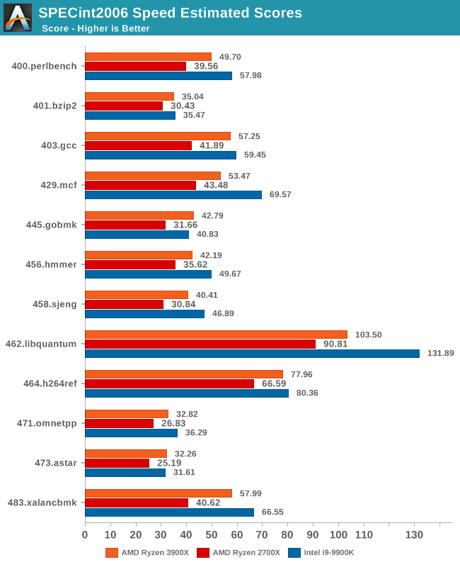
In terms of the int2006 benchmarks, the improvements of the new Zen2 based Ryzen 3900X is quite even across the board when compared to the Zen+ based Ryzen 2700X. We do note however somewhat larger performance increases in 403.gcc and 483.xalancbmk – it’s not immediately clear as to why as the benchmarks don’t have one particular characteristic that would fit Zen2’s design improvements, however I suspect it’s linked to the larger L3 cache.
445.gobmk in particular is a branch-heavy workload, and the 32% increase in performance here would be better explained by Zen2’s new additional TAGE branch predictor which is able to reduce overall branch misses.
It’s also interesting that although Ryzen3900X posted worse memory latency results than the 2700X, it’s still able to outperform the latter in memory sensitive workloads such as 429.mcf, although the increases for 471.omnetpp is amongst the smallest in the suite.
However we still see that AMD has an overall larger disadvantage to Intel in these memory sensitive tests, as the 9900K has large advantages in 429.mcf, and posting a large lead in the very memory bandwidth intensive 462.libquantum, the two tests that put the most pressure on the caches and memory subsystem.
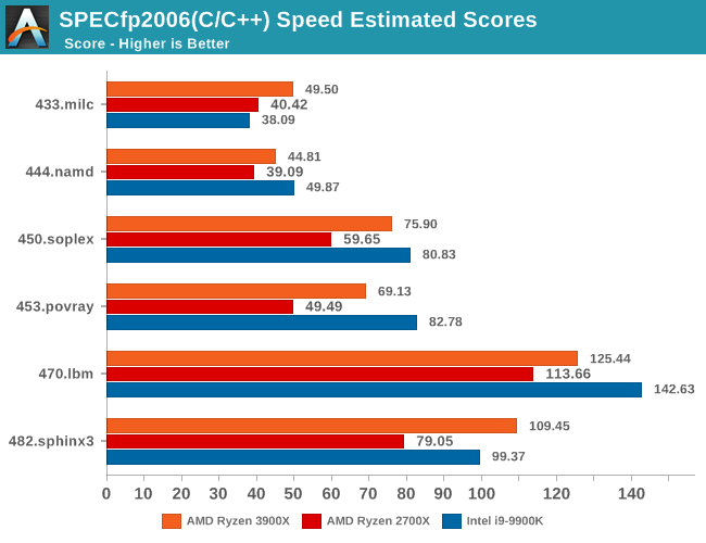
In the fp2006 benchmarks, we gain see some larger jumps on the part of the Ryzen 3900X, particularly in 482.sphinx3. These two tests along with 450.soplex are characterized by higher data cache misses, so Zen2’s 16MB L3 cache should definitely be part of the reason we see such larger jumps.
I found it interesting that we’re not seeing much improvements in 470.lbm even though this is a test that is data store heavy, so I would have expected Zen2’s additional store AGU to greatly benefit this workload. There must be some higher level memory limitations which is bottlenecking the test.
453.povray isn’t data heavy nor branch heavy, as it’s one of the more simple workloads in the suite. Here it’s mostly up to the execution backend throughput and the ability of the front-end to feed it fast enough that are the bottlenecks. So while the Ryzen 3900X provides a big boost over the 2700X, it’s still largely lagging behind the 9900K, a characteristic we’re also seeing in the similar execution bottlenecked 456.hmmer of the integer suite.
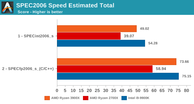
Overall, the 3900X is 20.8% faster in the integer and floating point tests of the SPEC2006 suite, which corresponds to a 13% IPC increase, the metric that AMD officially uses to promote the Zen2 microarchitectural increases.
Moving on to the 2017 suite, we have to clarify that we’re using the Rate benchmark variations. The 2017 suite’s speed and rate benchmarks differ from each other in terms of workloads. The speed tests were designed for single-threaded testing and have large memory demands of up to 11GB, while the rate tests were meant for multi-process tests. We’re using the rate variations of the benchmarks because we don’t see any large differentiation between the two variations in terms of their characterisation and thus the performance scaling between the both should be extremely similar. On top of that, the rate benchmarks take up to 5x less time (+1 hour vs +6 hours), on top of being able to run them on more memory limited platforms which we plan on to do in the future.
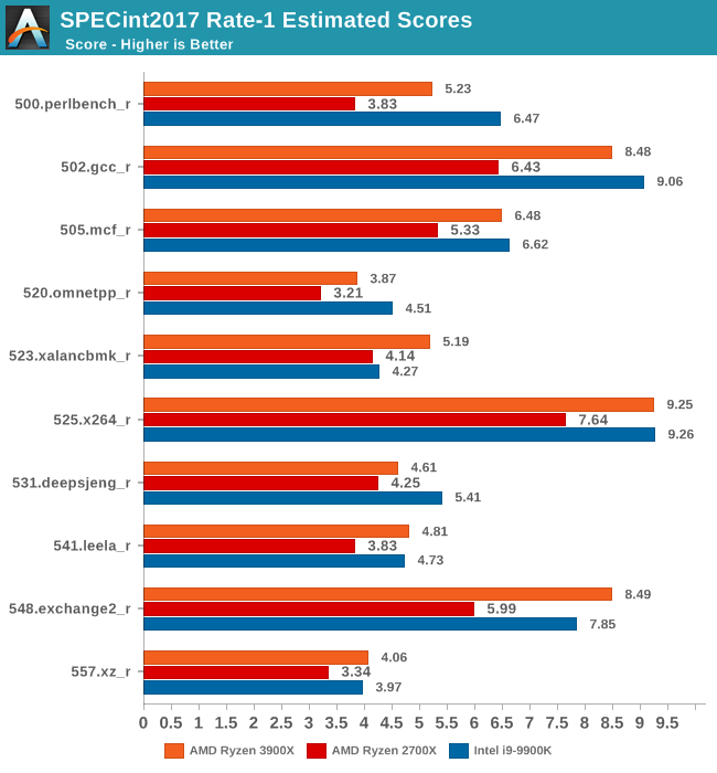
In the int2017 suite, we’re seeing similar performance differences and improvements, although this time around there’s a few workloads that are a bit more limited in terms of their performance boosts on the new Ryzen 3900X.
Unfortunately I’m not quite as familiar with the exact characteristics of these tests as I am with the 2006 suite, so a more detailed analysis should follow in the next few months as we delve deeper into microarchitectural counters.
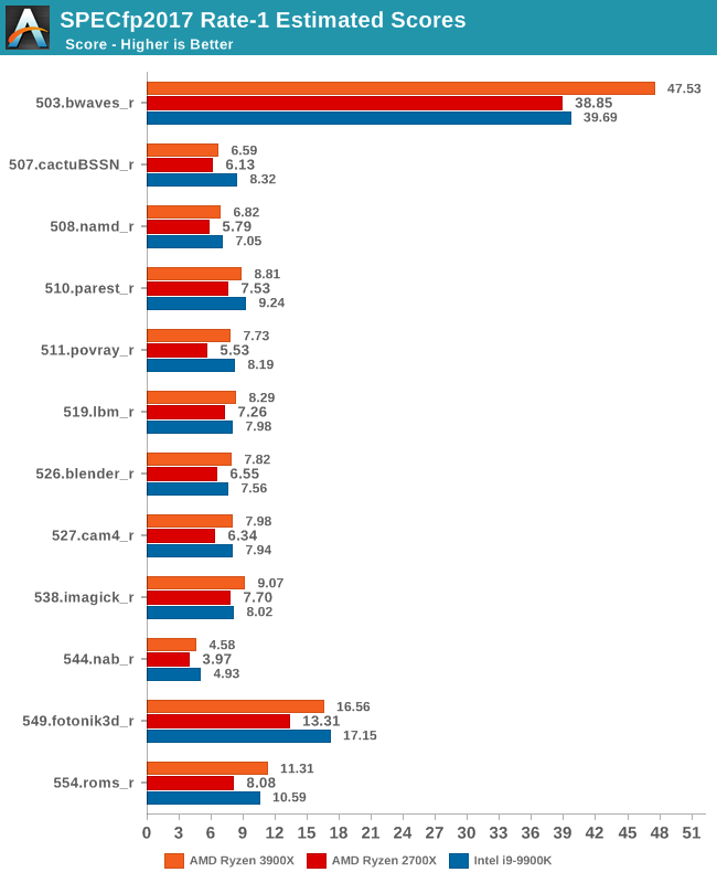
In the fp2017 suite, things are also quite even. Interesting enough here in particular AMD is able to leapfrog Intel’s 9900K in a lot more workloads, sometimes winning in terms of absolute performance and sometimes losing.
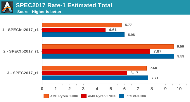
As for the overall performance scores, the new Ryzen 3900X improves by 18.1% over the 2700X. Although closing the gap greatly, it’s just shy of actually beating the 9900K’s absolute single-threaded performance.
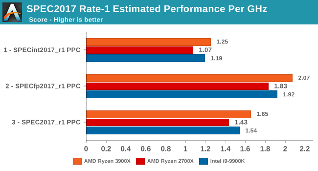
Normalising the scores for frequency, we see that AMD has achieved something that the company hasn’t been able to claim in over 15 years: It has beat Intel in terms of overall IPC. Overall here, the IPC improvements over Zen+ are 10.5%, which is a bit lower than the 13% figure for SPEC2006.
We already know about Intel’s new upcoming Sunny Cove microarchitecture which should undoubtedly be able to regain the IPC crown with relative ease, but the question for Intel is if they’ll be able to still maintain the single-thread absolute performance crown and continue to see 5GHz or similar clock speeds with the new core design.
While more the focus of low-end and small form factor systems, web-based benchmarks are notoriously difficult to standardize. Modern web browsers are frequently updated, with no recourse to disable those updates, and as such there is difficulty in keeping a common platform. The fast paced nature of browser development means that version numbers (and performance) can change from week to week. Despite this, web tests are often a good measure of user experience: a lot of what most office work is today revolves around web applications, particularly email and office apps, but also interfaces and development environments. Our web tests include some of the industry standard tests, as well as a few popular but older tests.
We have also included our legacy benchmarks in this section, representing a stack of older code for popular benchmarks.
All of our benchmark results can also be found in our benchmark engine, Bench.
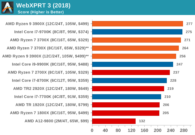
WebXPRT 3: Modern Real-World Web Tasks, including AI
The company behind the XPRT test suites, Principled Technologies, has recently released the latest web-test, and rather than attach a year to the name have just called it ‘3’. This latest test (as we started the suite) has built upon and developed the ethos of previous tests: user interaction, office compute, graph generation, list sorting, HTML5, image manipulation, and even goes as far as some AI testing.
For our benchmark, we run the standard test which goes through the benchmark list seven times and provides a final result. We run this standard test four times, and take an average.
Users can access the WebXPRT test at http://principledtechnologies.com/benchmarkxprt/webxprt/
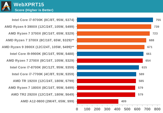
WebXPRT 2015: HTML5 and Javascript Web UX Testing
The older version of WebXPRT is the 2015 edition, which focuses on a slightly different set of web technologies and frameworks that are in use today. This is still a relevant test, especially for users interacting with not-the-latest web applications in the market, of which there are a lot. Web framework development is often very quick but with high turnover, meaning that frameworks are quickly developed, built-upon, used, and then developers move on to the next, and adjusting an application to a new framework is a difficult arduous task, especially with rapid development cycles. This leaves a lot of applications as ‘fixed-in-time’, and relevant to user experience for many years.
Similar to WebXPRT3, the main benchmark is a sectional run repeated seven times, with a final score. We repeat the whole thing four times, and average those final scores.
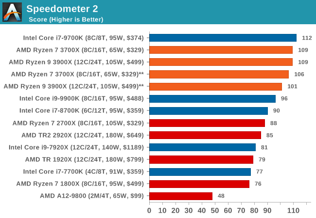
Speedometer 2: JavaScript Frameworks
Our newest web test is Speedometer 2, which is a accrued test over a series of javascript frameworks to do three simple things: built a list, enable each item in the list, and remove the list. All the frameworks implement the same visual cues, but obviously apply them from different coding angles.
Our test goes through the list of frameworks, and produces a final score indicative of ‘rpm’, one of the benchmarks internal metrics. We report this final score.
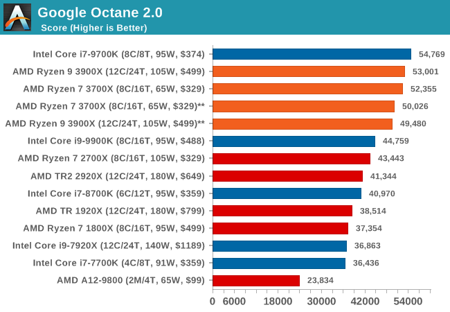
Google Octane 2.0: Core Web Compute
A popular web test for several years, but now no longer being updated, is Octane, developed by Google. Version 2.0 of the test performs the best part of two-dozen compute related tasks, such as regular expressions, cryptography, ray tracing, emulation, and Navier-Stokes physics calculations.
The test gives each sub-test a score and produces a geometric mean of the set as a final result. We run the full benchmark four times, and average the final results.
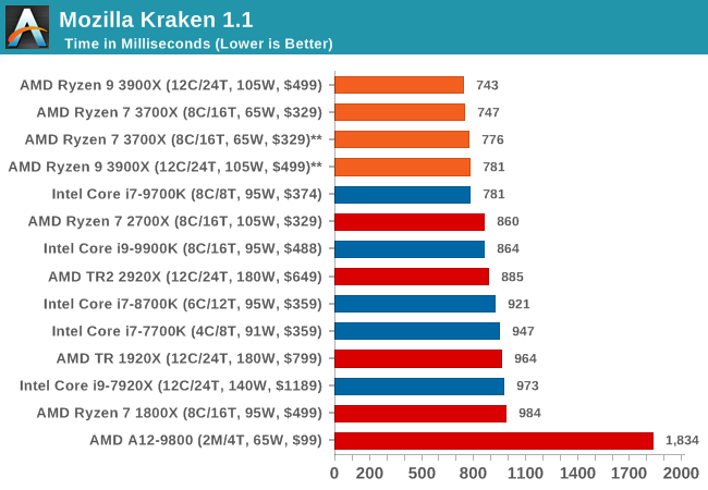
Mozilla Kraken 1.1: Core Web Compute
Even older than Octane is Kraken, this time developed by Mozilla. This is an older test that does similar computational mechanics, such as audio processing or image filtering. Kraken seems to produce a highly variable result depending on the browser version, as it is a test that is keenly optimized for.
The main benchmark runs through each of the sub-tests ten times and produces an average time to completion for each loop, given in milliseconds. We run the full benchmark four times and take an average of the time taken.
Web Tests Analysis
Overall, in the web tests, the new Ryzen 3900X and 3700X perform very well with both chips showcasing quite large improvements over the 2700X.
We’re seeing quite an interesting match-up against Intel’s 9700K here which is leading the all the benchmarks. The reason for this is that SKU has SMT turned off. The singe-threaded performance advantage of this is that the CPU core no longer has to share the µOP cache structure between to different threads, and has the whole capacity dedicated to one thread. Web workloads in particular are amongst the most instruction pressure heavy workloads out there, and they benefit extremely from turning SMT off on modern cores.
Whilst we didn’t have the time yet to test the new 3900X and 3700X with SMT off, AMD’s core and op cache works the same in that it’s sharing the capacity amongst two threads, statically partitioning it. I’m pretty sure we’d see larger increases in the web benchmarks when turning off SMT as well, and we’ll be sure to revisit this particular point in the future.
Our System Test section focuses significantly on real-world testing, user experience, with a slight nod to throughput. In this section we cover application loading time, image processing, simple scientific physics, emulation, neural simulation, optimized compute, and 3D model development, with a combination of readily available and custom software. For some of these tests, the bigger suites such as PCMark do cover them (we publish those values in our office section), although multiple perspectives is always beneficial. In all our tests we will explain in-depth what is being tested, and how we are testing.
All of our benchmark results can also be found in our benchmark engine, Bench.
Application Load: GIMP 2.10.4
One of the most important aspects about user experience and workflow is how fast does a system respond. A good test of this is to see how long it takes for an application to load. Most applications these days, when on an SSD, load fairly instantly, however some office tools require asset pre-loading before being available. Most operating systems employ caching as well, so when certain software is loaded repeatedly (web browser, office tools), then can be initialized much quicker.
In our last suite, we tested how long it took to load a large PDF in Adobe Acrobat. Unfortunately this test was a nightmare to program for, and didn’t transfer over to Win10 RS3 easily. In the meantime we discovered an application that can automate this test, and we put it up against GIMP, a popular free open-source online photo editing tool, and the major alternative to Adobe Photoshop. We set it to load a large 50MB design template, and perform the load 10 times with 10 seconds in-between each. Due to caching, the first 3-5 results are often slower than the rest, and time to cache can be inconsistent, we take the average of the last five results to show CPU processing on cached loading.
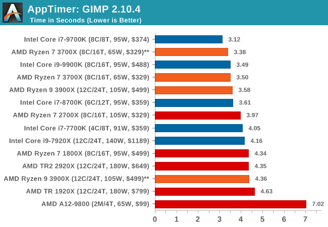
Application loading is typically single thread limited, but we see here that at some point it also becomes core-resource limited. Having access to more resources per thread in a non-HT environment helps the 8C/8T and 6C/6T processors get ahead of both of the 5.0 GHz parts in our testing.
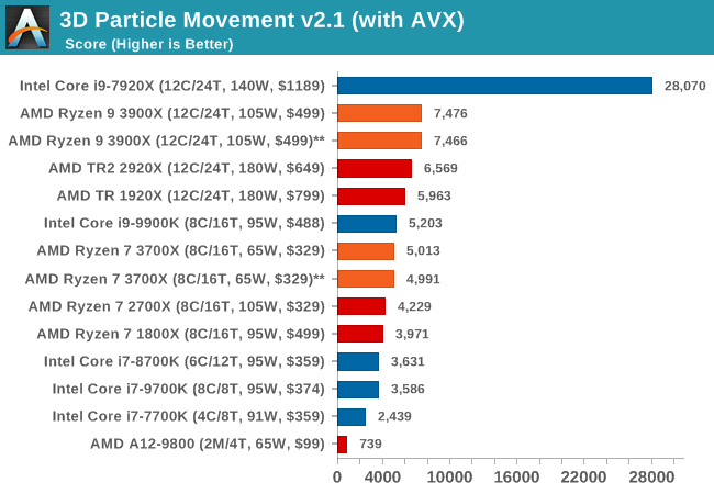
3D Particle Movement v2.1: Brownian Motion
Our 3DPM test is a custom built benchmark designed to simulate six different particle movement algorithms of points in a 3D space. The algorithms were developed as part of my PhD., and while ultimately perform best on a GPU, provide a good idea on how instruction streams are interpreted by different microarchitectures.
A key part of the algorithms is the random number generation – we use relatively fast generation which ends up implementing dependency chains in the code. The upgrade over the naïve first version of this code solved for false sharing in the caches, a major bottleneck. We are also looking at AVX2 and AVX512 versions of this benchmark for future reviews.
For this test, we run a stock particle set over the six algorithms for 20 seconds apiece, with 10 second pauses, and report the total rate of particle movement, in millions of operations (movements) per second. We have a non-AVX version and an AVX version, with the latter implementing AVX512 and AVX2 where possible.
3DPM v2.1 can be downloaded from our server: 3DPMv2.1.rar (13.0 MB)
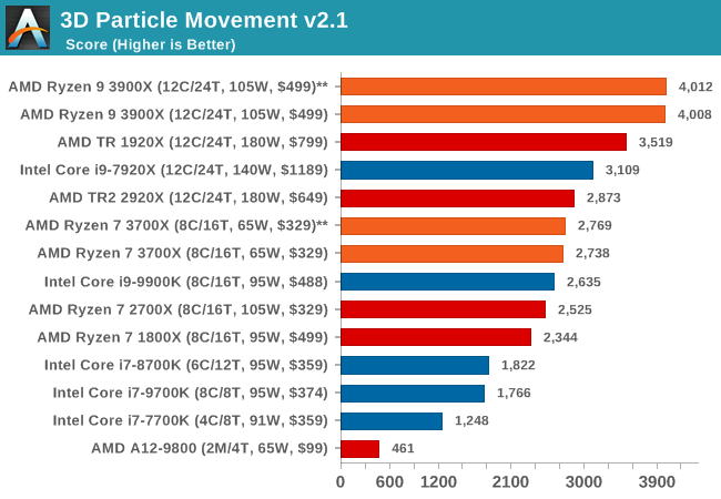
With a non-AVX code base, the 9900K shows the IPC and frequency improvements over the R7 2700X, although in reality it is not as big of a percentage jump as you might imagine. The processors without HT get pushed back a bit here.
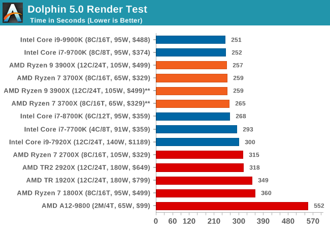
Dolphin 5.0: Console Emulation
One of the popular requested tests in our suite is to do with console emulation. Being able to pick up a game from an older system and run it as expected depends on the overhead of the emulator: it takes a significantly more powerful x86 system to be able to accurately emulate an older non-x86 console, especially if code for that console was made to abuse certain physical bugs in the hardware.
For our test, we use the popular Dolphin emulation software, and run a compute project through it to determine how close to a standard console system our processors can emulate. In this test, a Nintendo Wii would take around 1050 seconds.
The latest version of Dolphin can be downloaded from https://dolphin-emu.org/
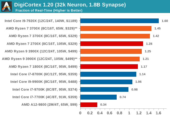
DigiCortex 1.20: Sea Slug Brain Simulation
This benchmark was originally designed for simulation and visualization of neuron and synapse activity, as is commonly found in the brain. The software comes with a variety of benchmark modes, and we take the small benchmark which runs a 32k neuron / 1.8B synapse simulation, equivalent to a Sea Slug.

Example of a 2.1B neuron simulation
We report the results as the ability to simulate the data as a fraction of real-time, so anything above a ‘one’ is suitable for real-time work. Out of the two modes, a ‘non-firing’ mode which is DRAM heavy and a ‘firing’ mode which has CPU work, we choose the latter. Despite this, the benchmark is still affected by DRAM speed a fair amount.
DigiCortex can be downloaded from http://www.digicortex.net/
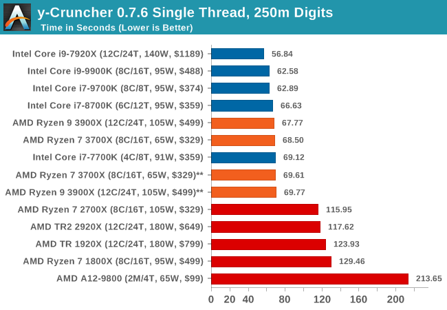
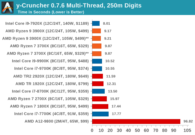
y-Cruncher v0.7.6: Microarchitecture Optimized Compute
I’ve known about y-Cruncher for a while, as a tool to help compute various mathematical constants, but it wasn’t until I began talking with its developer, Alex Yee, a researcher from NWU and now software optimization developer, that I realized that he has optimized the software like crazy to get the best performance. Naturally, any simulation that can take 20+ days can benefit from a 1% performance increase! Alex started y-cruncher as a high-school project, but it is now at a state where Alex is keeping it up to date to take advantage of the latest instruction sets before they are even made available in hardware.
For our test we run y-cruncher v0.7.6 through all the different optimized variants of the binary, single threaded and multi-threaded, including the AVX-512 optimized binaries. The test is to calculate 250m digits of Pi, and we use the single threaded and multi-threaded versions of this test.
Users can download y-cruncher from Alex’s website: http://www.numberworld.org/y-cruncher/
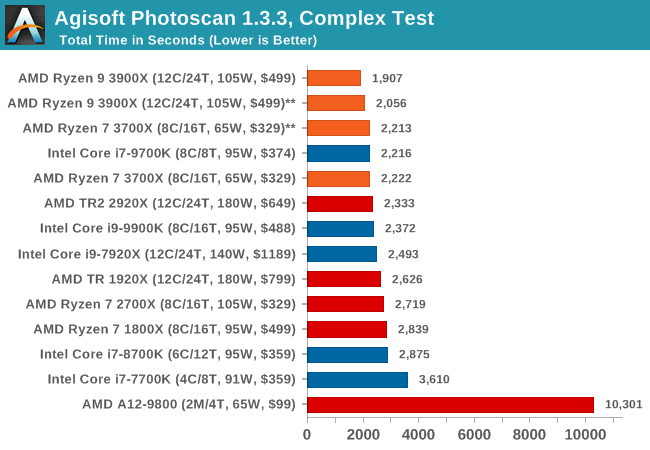
Agisoft Photoscan 1.3.3: 2D Image to 3D Model Conversion
One of the ISVs that we have worked with for a number of years is Agisoft, who develop software called PhotoScan that transforms a number of 2D images into a 3D model. This is an important tool in model development and archiving, and relies on a number of single threaded and multi-threaded algorithms to go from one side of the computation to the other.
In our test, we take v1.3.3 of the software with a good sized data set of 84 x 18 megapixel photos and push it through a reasonably fast variant of the algorithms, but is still more stringent than our 2017 test. We report the total time to complete the process.
Agisoft’s Photoscan website can be found here: http://www.agisoft.com/
Rendering is often a key target for processor workloads, lending itself to a professional environment. It comes in different formats as well, from 3D rendering through rasterization, such as games, or by ray tracing, and invokes the ability of the software to manage meshes, textures, collisions, aliasing, physics (in animations), and discarding unnecessary work. Most renderers offer CPU code paths, while a few use GPUs and select environments use FPGAs or dedicated ASICs. For big studios however, CPUs are still the hardware of choice.
All of our benchmark results can also be found in our benchmark engine, Bench.
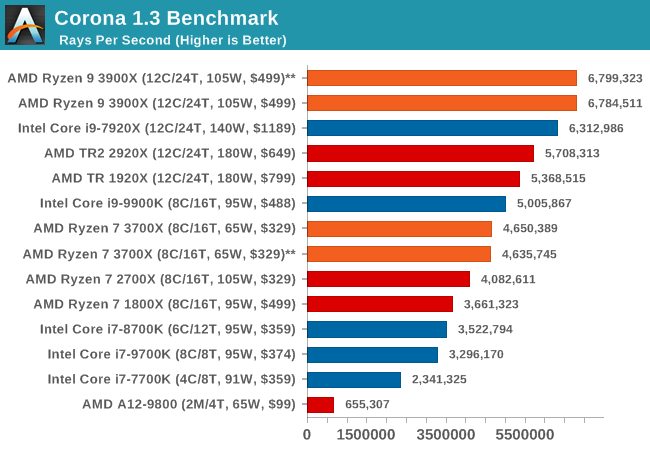
Corona 1.3: Performance Render
An advanced performance based renderer for software such as 3ds Max and Cinema 4D, the Corona benchmark renders a generated scene as a standard under its 1.3 software version. Normally the GUI implementation of the benchmark shows the scene being built, and allows the user to upload the result as a ‘time to complete’.
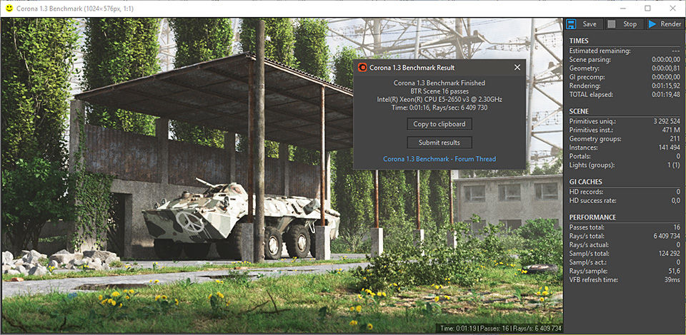
We got in contact with the developer who gave us a command line version of the benchmark that does a direct output of results. Rather than reporting time, we report the average number of rays per second across six runs, as the performance scaling of a result per unit time is typically visually easier to understand.
The Corona benchmark website can be found at https://corona-renderer.com/benchmark
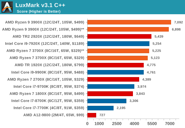
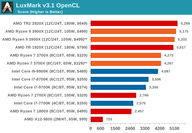
LuxMark v3.1: LuxRender via Different Code Paths
As stated at the top, there are many different ways to process rendering data: CPU, GPU, Accelerator, and others. On top of that, there are many frameworks and APIs in which to program, depending on how the software will be used. LuxMark, a benchmark developed using the LuxRender engine, offers several different scenes and APIs.
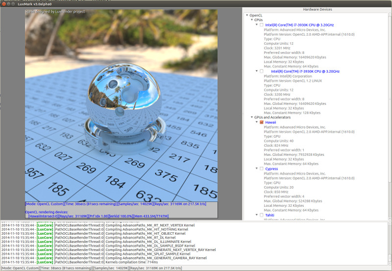
Taken from the Linux Version of LuxMark
In our test, we run the simple ‘Ball’ scene on both the C++ and OpenCL code paths, but in CPU mode. This scene starts with a rough render and slowly improves the quality over two minutes, giving a final result in what is essentially an average ‘kilorays per second’.
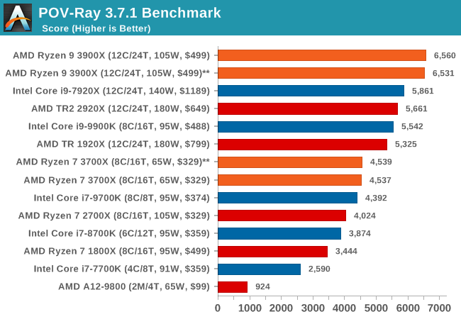
POV-Ray 3.7.1: Ray Tracing
The Persistence of Vision ray tracing engine is another well-known benchmarking tool, which was in a state of relative hibernation until AMD released its Zen processors, to which suddenly both Intel and AMD were submitting code to the main branch of the open source project. For our test, we use the built-in benchmark for all-cores, called from the command line.
POV-Ray can be downloaded from http://www.povray.org/
With the rise of streaming, vlogs, and video content as a whole, encoding and transcoding tests are becoming ever more important. Not only are more home users and gamers needing to convert video files into something more manageable, for streaming or archival purposes, but the servers that manage the output also manage around data and log files with compression and decompression. Our encoding tasks are focused around these important scenarios, with input from the community for the best implementation of real-world testing.
All of our benchmark results can also be found in our benchmark engine, Bench.
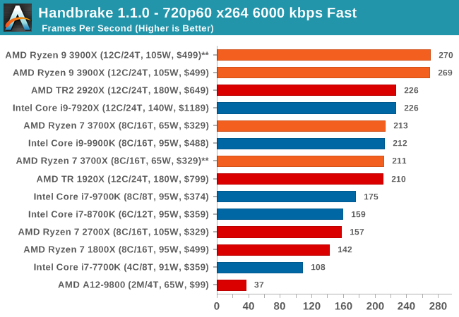
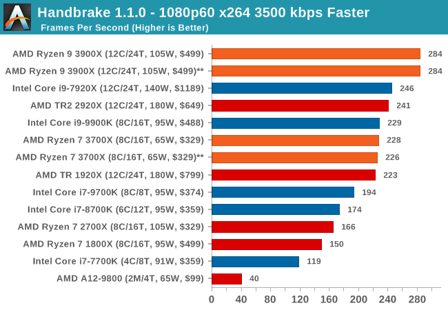
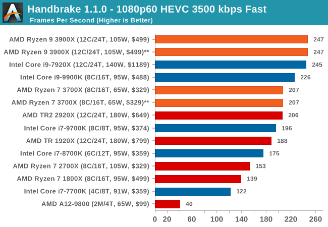
Handbrake 1.1.0: Streaming and Archival Video Transcoding
A popular open source tool, Handbrake is the anything-to-anything video conversion software that a number of people use as a reference point. The danger is always on version numbers and optimization, for example the latest versions of the software can take advantage of AVX-512 and OpenCL to accelerate certain types of transcoding and algorithms. The version we use here is a pure CPU play, with common transcoding variations.
We have split Handbrake up into several tests, using a Logitech C920 1080p60 native webcam recording (essentially a streamer recording), and convert them into two types of streaming formats and one for archival. The output settings used are:
- 720p60 at 6000 kbps constant bit rate, fast setting, high profile
- 1080p60 at 3500 kbps constant bit rate, faster setting, main profile
- 1080p60 HEVC at 3500 kbps variable bit rate, fast setting, main profile
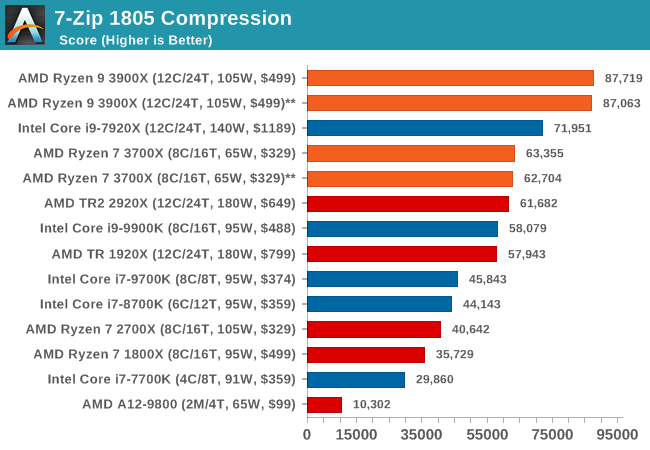
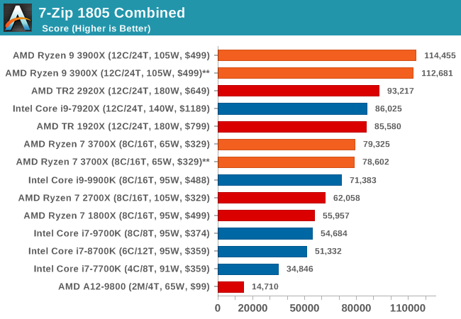
7-zip v1805: Popular Open-Source Encoding Engine
Out of our compression/decompression tool tests, 7-zip is the most requested and comes with a built-in benchmark. For our test suite, we’ve pulled the latest version of the software and we run the benchmark from the command line, reporting the compression, decompression, and a combined score.
It is noted in this benchmark that the latest multi-die processors have very bi-modal performance between compression and decompression, performing well in one and badly in the other. There are also discussions around how the Windows Scheduler is implementing every thread. As we get more results, it will be interesting to see how this plays out.
Please note, if you plan to share out the Compression graph, please include the Decompression one. Otherwise you’re only presenting half a picture.

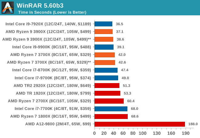
WinRAR 5.60b3: Archiving Tool
My compression tool of choice is often WinRAR, having been one of the first tools a number of my generation used over two decades ago. The interface has not changed much, although the integration with Windows right click commands is always a plus. It has no in-built test, so we run a compression over a set directory containing over thirty 60-second video files and 2000 small web-based files at a normal compression rate.
WinRAR is variable threaded but also susceptible to caching, so in our test we run it 10 times and take the average of the last five, leaving the test purely for raw CPU compute performance.
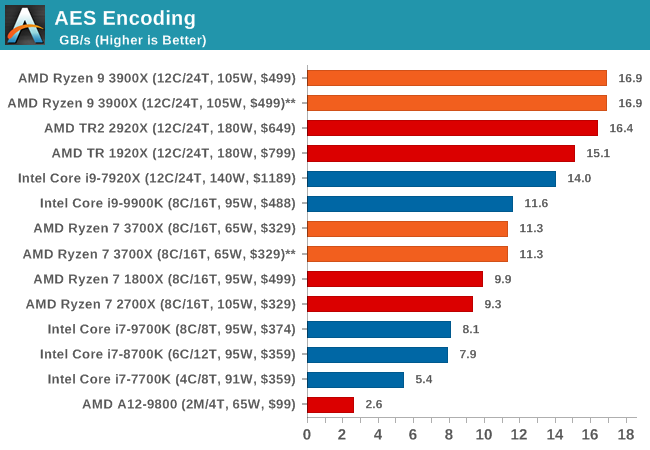
AES Encryption: File Security
A number of platforms, particularly mobile devices, are now offering encryption by default with file systems in order to protect the contents. Windows based devices have these options as well, often applied by BitLocker or third-party software. In our AES encryption test, we used the discontinued TrueCrypt for its built-in benchmark, which tests several encryption algorithms directly in memory.
The data we take for this test is the combined AES encrypt/decrypt performance, measured in gigabytes per second. The software does use AES commands for processors that offer hardware selection, however not AVX-512.
The Office test suite is designed to focus around more industry standard tests that focus on office workflows, system meetings, some synthetics, but we also bundle compiler performance in with this section. For users that have to evaluate hardware in general, these are usually the benchmarks that most consider.
All of our benchmark results can also be found in our benchmark engine, Bench.
PCMark 10: Industry Standard System Profiler
Futuremark, now known as UL, has developed benchmarks that have become industry standards for around two decades. The latest complete system test suite is PCMark 10, upgrading over PCMark 8 with updated tests and more OpenCL invested into use cases such as video streaming.
PCMark splits its scores into about 14 different areas, including application startup, web, spreadsheets, photo editing, rendering, video conferencing, and physics. We post all of these numbers in our benchmark database, Bench, however the key metric for the review is the overall score.
We're investigating the PCMark results, which seem abnormally high.
3DMark Physics: In-Game Physics Compute
Alongside PCMark is 3DMark, Futuremark’s (UL’s) gaming test suite. Each gaming tests consists of one or two GPU heavy scenes, along with a physics test that is indicative of when the test was written and the platform it is aimed at. The main overriding tests, in order of complexity, are Ice Storm, Cloud Gate, Sky Diver, Fire Strike, and Time Spy.
Some of the subtests offer variants, such as Ice Storm Unlimited, which is aimed at mobile platforms with an off-screen rendering, or Fire Strike Ultra which is aimed at high-end 4K systems with lots of the added features turned on. Time Spy also currently has an AVX-512 mode (which we may be using in the future).
For our tests, we report in Bench the results from every physics test, but for the sake of the review we keep it to the most demanding of each scene: Ice Storm Unlimited, Cloud Gate, Sky Diver, Fire Strike Ultra, and Time Spy.
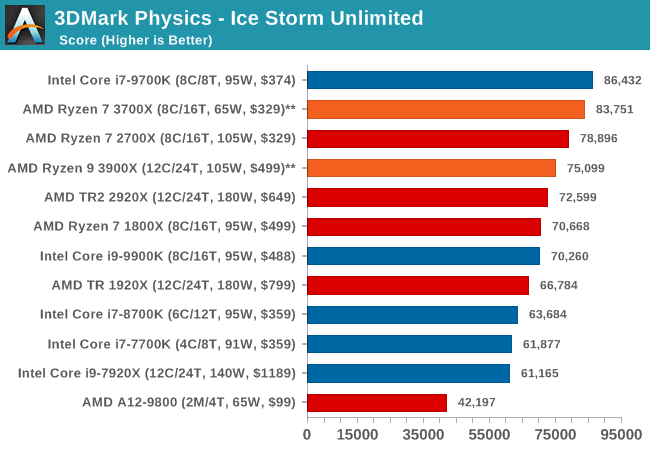
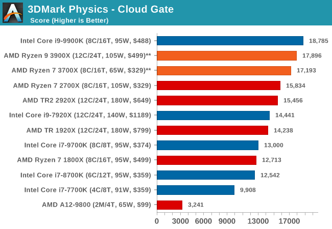
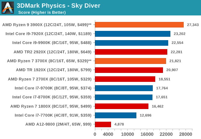
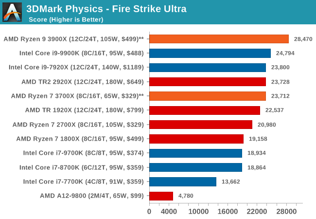
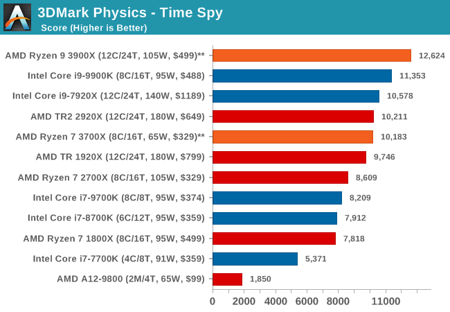
The older Ice Storm test didn't much like the Core i9-9900K, pushing it back behind the R7 1800X. For the more modern tests focused on PCs, the 9900K wins out. The lack of HT is hurting the other two parts.
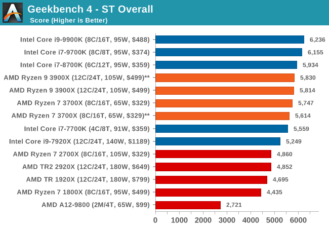
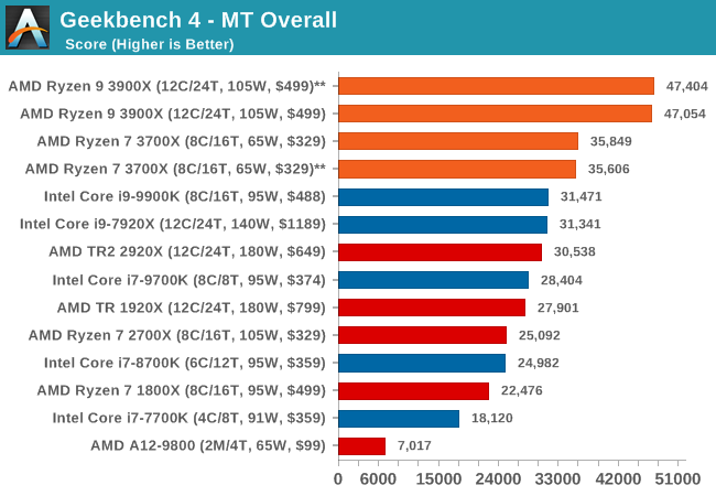
GeekBench4: Synthetics
A common tool for cross-platform testing between mobile, PC, and Mac, GeekBench 4 is an ultimate exercise in synthetic testing across a range of algorithms looking for peak throughput. Tests include encryption, compression, fast Fourier transform, memory operations, n-body physics, matrix operations, histogram manipulation, and HTML parsing.
I’m including this test due to popular demand, although the results do come across as overly synthetic, and a lot of users often put a lot of weight behind the test due to the fact that it is compiled across different platforms (although with different compilers).
We record the main subtest scores (Crypto, Integer, Floating Point, Memory) in our benchmark database, but for the review we post the overall single and multi-threaded results.
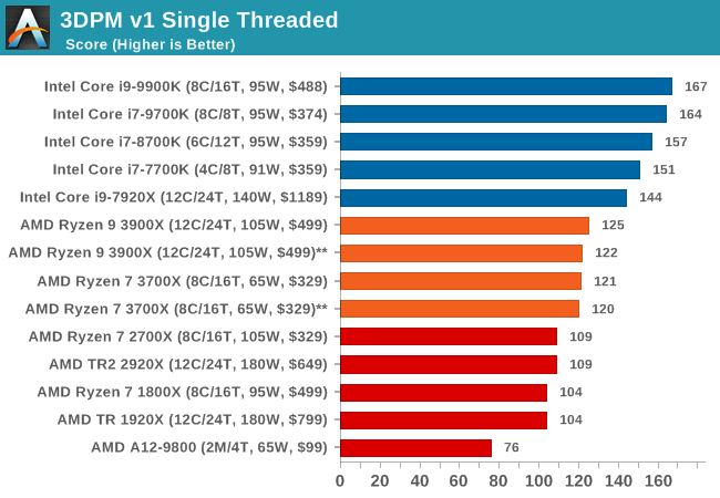
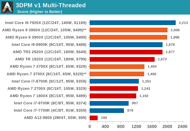
3DPM v1: Naïve Code Variant of 3DPM v2.1
The first legacy test in the suite is the first version of our 3DPM benchmark. This is the ultimate naïve version of the code, as if it was written by scientist with no knowledge of how computer hardware, compilers, or optimization works (which in fact, it was at the start). This represents a large body of scientific simulation out in the wild, where getting the answer is more important than it being fast (getting a result in 4 days is acceptable if it’s correct, rather than sending someone away for a year to learn to code and getting the result in 5 minutes).
In this version, the only real optimization was in the compiler flags (-O2, -fp:fast), compiling it in release mode, and enabling OpenMP in the main compute loops. The loops were not configured for function size, and one of the key slowdowns is false sharing in the cache. It also has long dependency chains based on the random number generation, which leads to relatively poor performance on specific compute microarchitectures.
3DPM v1 can be downloaded with our 3DPM v2 code here: 3DPMv2.1.rar (13.0 MB)
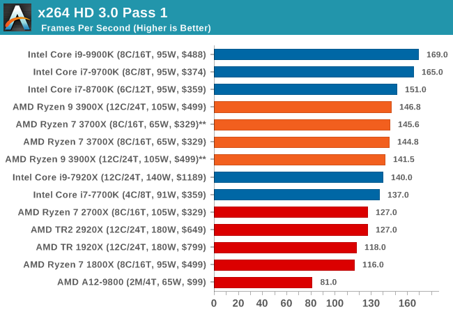
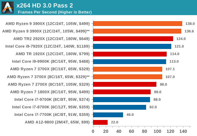
x264 HD 3.0: Older Transcode Test
This transcoding test is super old, and was used by Anand back in the day of Pentium 4 and Athlon II processors. Here a standardized 720p video is transcoded with a two-pass conversion, with the benchmark showing the frames-per-second of each pass. This benchmark is single-threaded, and between some micro-architectures we seem to actually hit an instructions-per-clock wall.
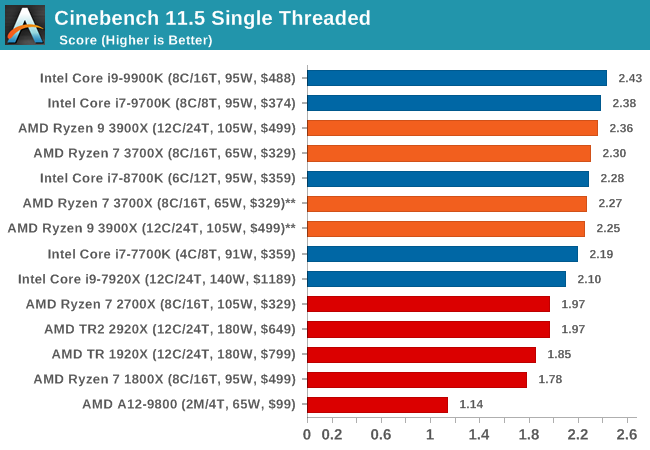
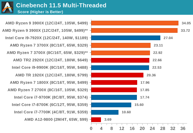
CineBench 11.5 and 10
Cinebench is a widely known benchmarking tool for measuring performance relative to MAXON's animation software Cinema 4D. Cinebench has been optimized over a decade and focuses on purely CPU horsepower, meaning if there is a discrepancy in pure throughput characteristics, Cinebench is likely to show that discrepancy. Arguably other software doesn't make use of all the tools available, so the real world relevance might purely be academic, but given our large database of data for Cinebench it seems difficult to ignore a small five minute test. We run the modern version 15 in this test, as well as the older 11.5 due to our back data.
Albeit different to most of the other commonly played MMO or massively multiplayer online games, World of Tanks is set in the mid-20th century and allows players to take control of a range of military based armored vehicles. World of Tanks (WoT) is developed and published by Wargaming who are based in Belarus, with the game’s soundtrack being primarily composed by Belarusian composer Sergey Khmelevsky. The game offers multiple entry points including a free-to-play element as well as allowing players to pay a fee to open up more features. One of the most interesting things about this tank based MMO is that it achieved eSports status when it debuted at the World Cyber Games back in 2012.

World of Tanks enCore is a demo application for a new and unreleased graphics engine penned by the Wargaming development team. Over time the new core engine will implemented into the full game upgrading the games visuals with key elements such as improved water, flora, shadows, lighting as well as other objects such as buildings. The World of Tanks enCore demo app not only offers up insight into the impending game engine changes, but allows users to check system performance to see if the new engine run optimally on their system.
| AnandTech CPU Gaming 2019 Game List | ||||||||
| Game | Genre | Release Date | API | IGP | Low | Med | High | |
| World of Tanks enCore | Driving / Action | Feb 2018 |
DX11 | 768p Minimum |
1080p Medium |
1080p Ultra |
4K Ultra |
|
All of our benchmark results can also be found in our benchmark engine, Bench.

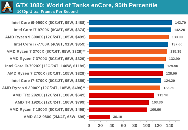
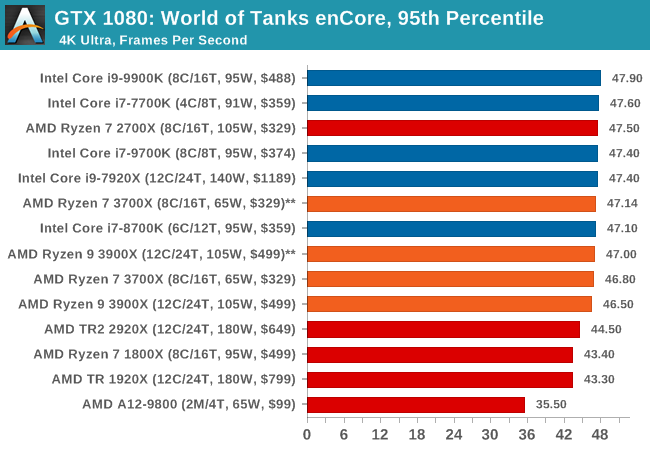
| World of Tanks enCore | IGP | Low | Medium | High |
| Average FPS | |
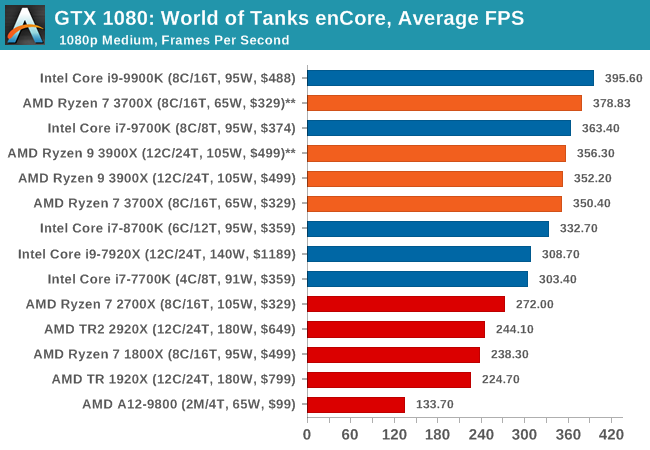 |
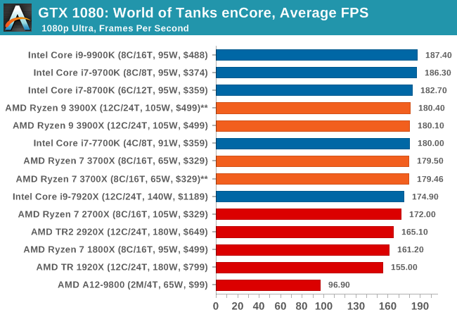 |
 |
| 95th Percentile | 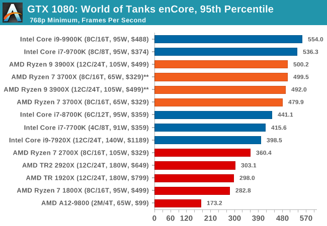 |
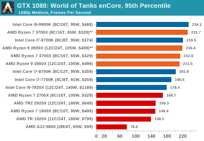 |
 |
 |
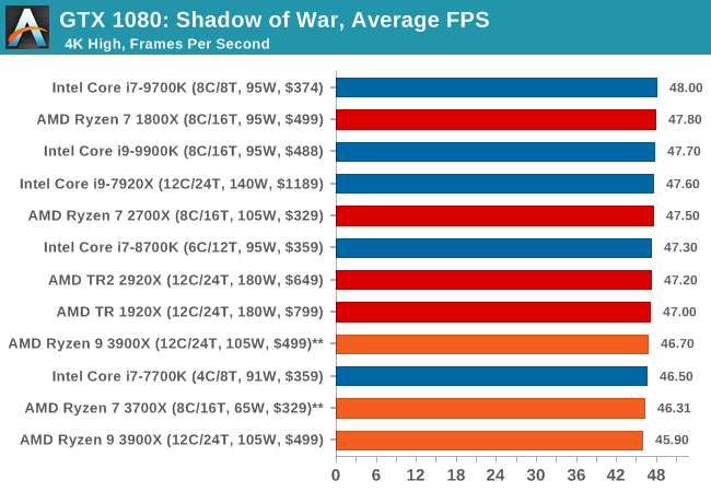
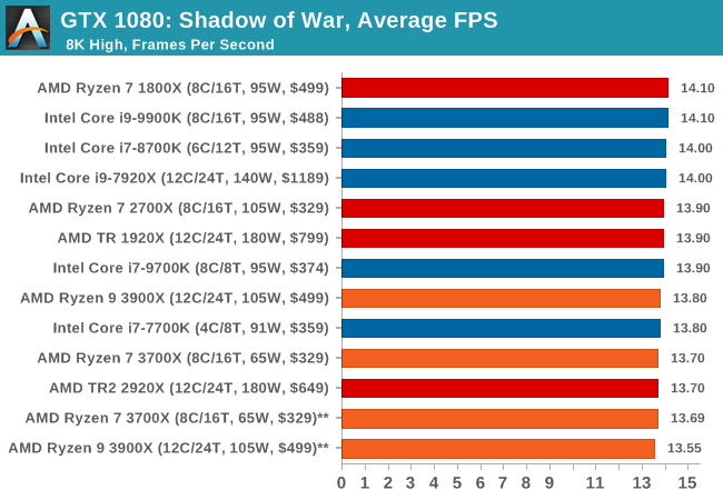
Next up is Middle-earth: Shadow of War, the sequel to Shadow of Mordor. Developed by Monolith, whose last hit was arguably F.E.A.R., Shadow of Mordor returned them to the spotlight with an innovative NPC rival generation and interaction system called the Nemesis System, along with a storyline based on J.R.R. Tolkien's legendarium, and making it work on a highly modified engine that originally powered F.E.A.R. in 2005.

Using the new LithTech Firebird engine, Shadow of War improves on the detail and complexity, and with free add-on high-resolution texture packs, offers itself as a good example of getting the most graphics out of an engine that may not be bleeding edge. Shadow of War also supports HDR (HDR10).
| AnandTech CPU Gaming 2019 Game List | ||||||||
| Game | Genre | Release | API | IGP | Low | Med | High | |
| Shadow of War | Action / RPG | Sep 2017 | DX11 | 720p Ultra | 1080p Ultra | 4K High | 8K High | |
All of our benchmark results can also be found in our benchmark engine, Bench.
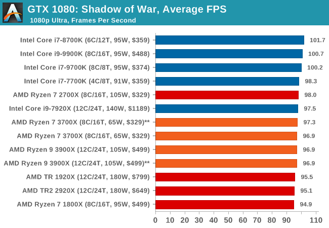
| Shadow of War | IGP | Low | Medium | High |
| Average FPS | 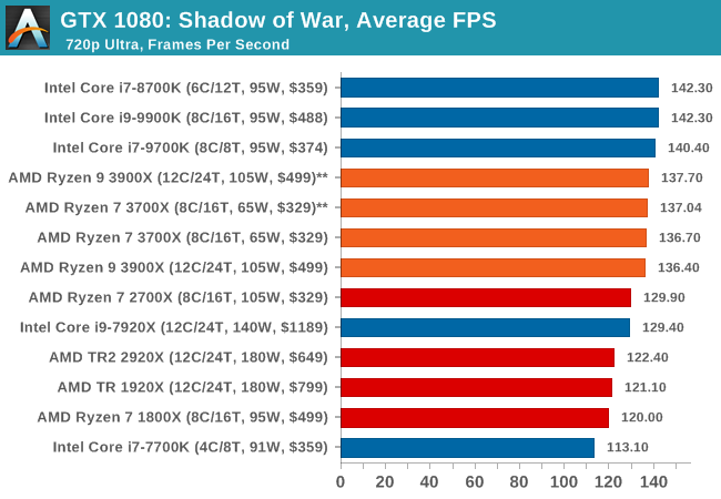 |
|
 |
 |
Seen as the holy child of DirectX12, Ashes of the Singularity (AoTS, or just Ashes) has been the first title to actively go explore as many of the DirectX12 features as it possibly can. Stardock, the developer behind the Nitrous engine which powers the game, has ensured that the real-time strategy title takes advantage of multiple cores and multiple graphics cards, in as many configurations as possible.
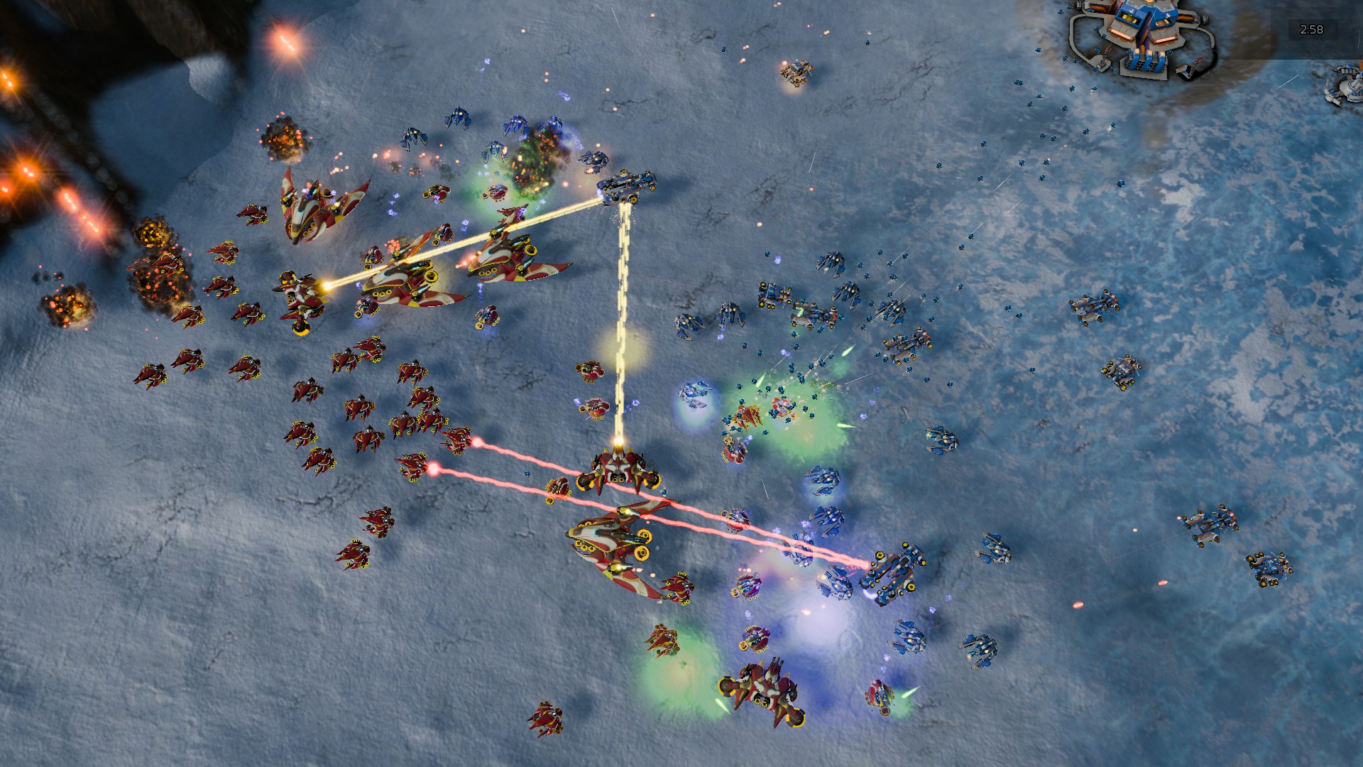
As a real-time strategy title, Ashes is all about responsiveness during both wide open shots but also concentrated battles. With DirectX12 at the helm, the ability to implement more draw calls per second allows the engine to work with substantial unit depth and effects that other RTS titles had to rely on combined draw calls to achieve, making some combined unit structures ultimately very rigid.
Stardock clearly understand the importance of an in-game benchmark, ensuring that such a tool was available and capable from day one, especially with all the additional DX12 features used and being able to characterize how they affected the title for the developer was important. The in-game benchmark performs a four minute fixed seed battle environment with a variety of shots, and outputs a vast amount of data to analyze.
For our benchmark, we run Ashes Classic: an older version of the game before the Escalation update. The reason for this is that this is easier to automate, without a splash screen, but still has a strong visual fidelity to test.
| AnandTech CPU Gaming 2019 Game List | ||||||||
| Game | Genre | Release Date | API | IGP | Low | Med | High | |
| Ashes: Classic | RTS | Mar 2016 |
DX12 | 720p Standard |
1080p Standard |
1440p Standard |
4K Standard |
|
Ashes has dropdown options for MSAA, Light Quality, Object Quality, Shading Samples, Shadow Quality, Textures, and separate options for the terrain. There are several presents, from Very Low to Extreme: we run our benchmarks at the above settings, and take the frame-time output for our average and percentile numbers.
All of our benchmark results can also be found in our benchmark engine, Bench.
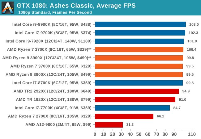
| Ashes Classic | IGP | Low | Medium | High |
| Average FPS | 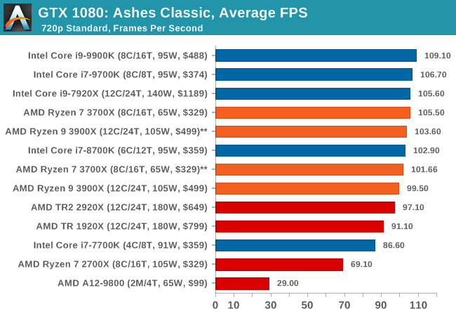 |
|
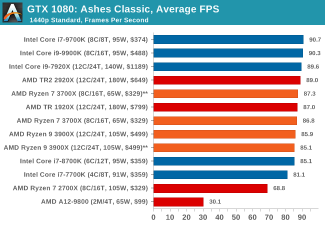 |
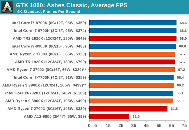 |
| 95th Percentile | 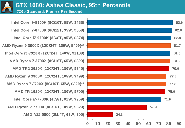 |
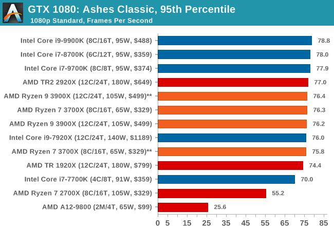 |
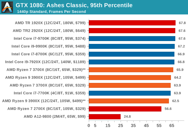 |
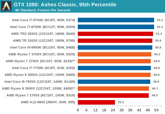 |
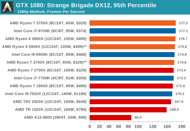
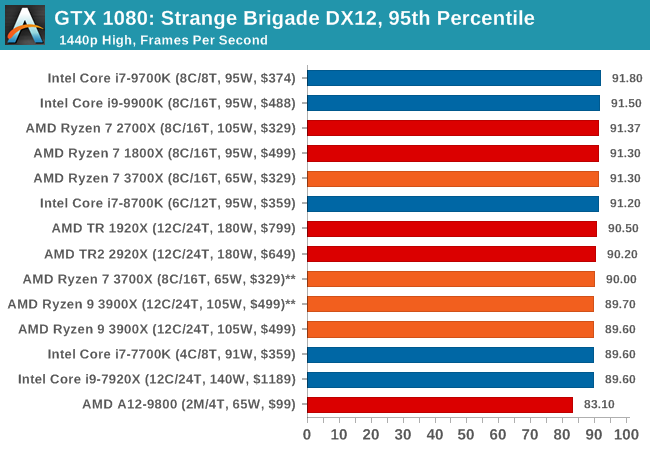
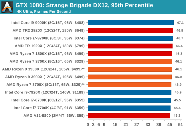
Strange Brigade is based in 1903’s Egypt and follows a story which is very similar to that of the Mummy film franchise. This particular third-person shooter is developed by Rebellion Developments which is more widely known for games such as the Sniper Elite and Alien vs Predator series. The game follows the hunt for Seteki the Witch Queen who has arose once again and the only ‘troop’ who can ultimately stop her. Gameplay is cooperative centric with a wide variety of different levels and many puzzles which need solving by the British colonial Secret Service agents sent to put an end to her reign of barbaric and brutality.

The game supports both the DirectX 12 and Vulkan APIs and houses its own built-in benchmark which offers various options up for customization including textures, anti-aliasing, reflections, draw distance and even allows users to enable or disable motion blur, ambient occlusion and tessellation among others. AMD has boasted previously that Strange Brigade is part of its Vulkan API implementation offering scalability for AMD multi-graphics card configurations.
| AnandTech CPU Gaming 2019 Game List | ||||||||
| Game | Genre | Release Date | API | IGP | Low | Med | High | |
| Strange Brigade* | FPS | Aug 2018 |
DX12 Vulkan |
720p Low |
1080p Medium |
1440p High |
4K Ultra |
|
| *Strange Brigade is run in DX12 and Vulkan modes | ||||||||
All of our benchmark results can also be found in our benchmark engine, Bench.
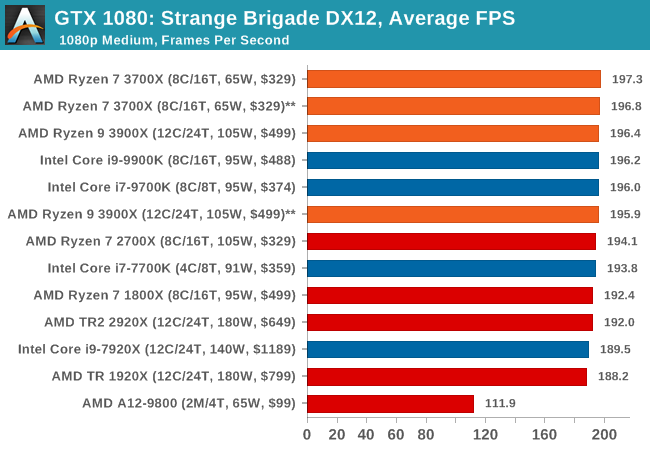
| Strange Brigade DX12 | IGP | Low | Medium | High |
| Average FPS | 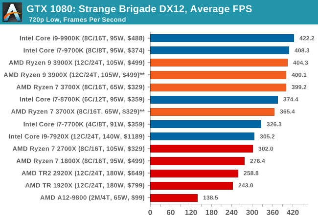 |
|
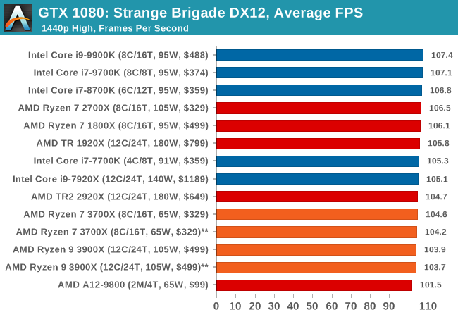 |
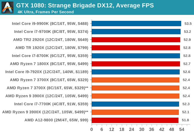 |
| 95th Percentile | 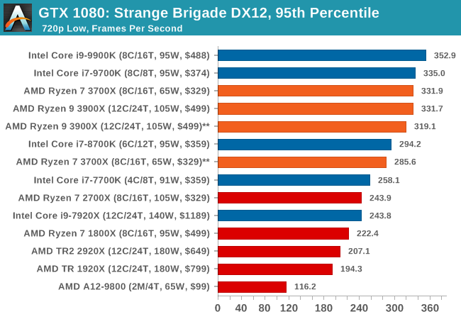 |
 |
 |
 |
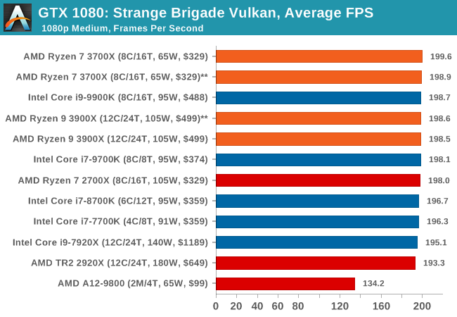
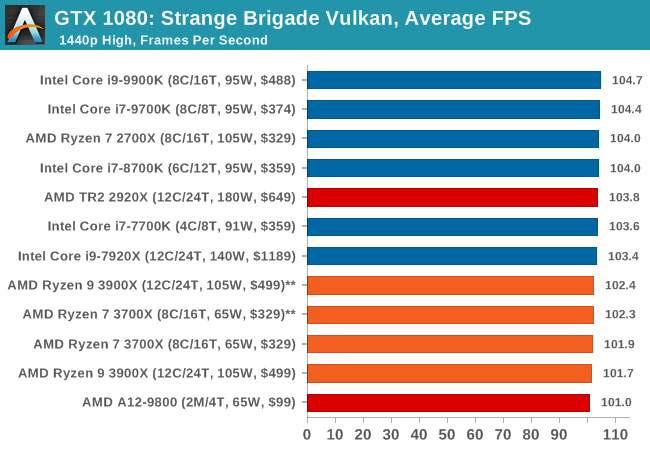
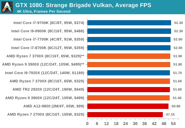
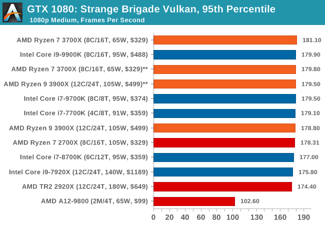
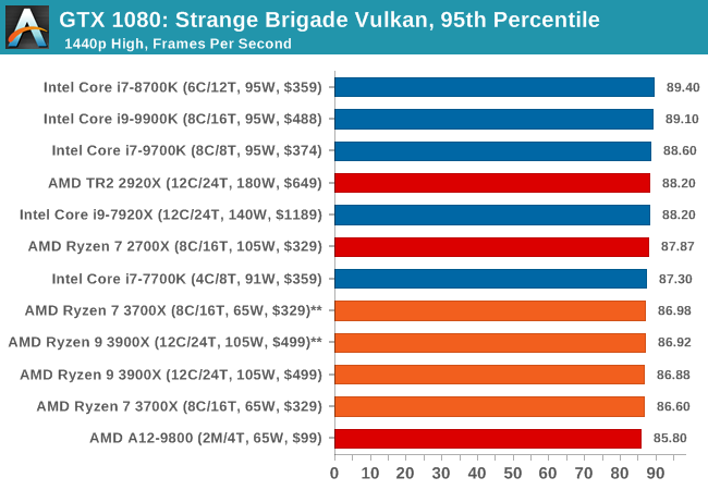
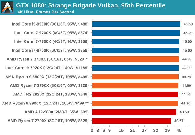
| Strange Brigade Vulkan | IGP | Low | Medium | High |
| Average FPS | 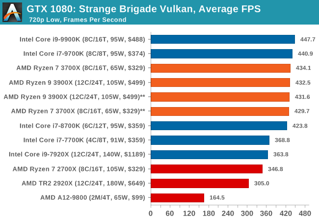 |
|
 |
 |
| 95th Percentile | 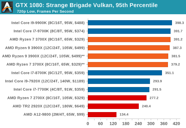 |
 |
 |
 |
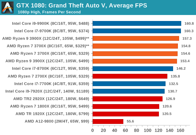
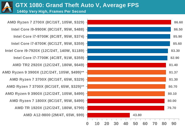
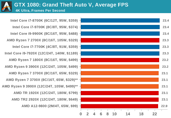
The highly anticipated iteration of the Grand Theft Auto franchise hit the shelves on April 14th 2015, with both AMD and NVIDIA in tow to help optimize the title. GTA doesn’t provide graphical presets, but opens up the options to users and extends the boundaries by pushing even the hardest systems to the limit using Rockstar’s Advanced Game Engine under DirectX 11. Whether the user is flying high in the mountains with long draw distances or dealing with assorted trash in the city, when cranked up to maximum it creates stunning visuals but hard work for both the CPU and the GPU.
For our test we have scripted a version of the in-game benchmark. The in-game benchmark consists of five scenarios: four short panning shots with varying lighting and weather effects, and a fifth action sequence that lasts around 90 seconds. We use only the final part of the benchmark, which combines a flight scene in a jet followed by an inner city drive-by through several intersections followed by ramming a tanker that explodes, causing other cars to explode as well. This is a mix of distance rendering followed by a detailed near-rendering action sequence, and the title thankfully spits out frame time data.
| AnandTech CPU Gaming 2019 Game List | ||||||||
| Game | Genre | Release Date | API | IGP | Low | Med | High | |
| Grand Theft Auto V | Open World | Apr 2015 |
DX11 | 720p Low |
1080p High |
1440p Very High |
4K Ultra |
|
| *Strange Brigade is run in DX12 and Vulkan modes | ||||||||
There are no presets for the graphics options on GTA, allowing the user to adjust options such as population density and distance scaling on sliders, but others such as texture/shadow/shader/water quality from Low to Very High. Other options include MSAA, soft shadows, post effects, shadow resolution and extended draw distance options. There is a handy option at the top which shows how much video memory the options are expected to consume, with obvious repercussions if a user requests more video memory than is present on the card (although there’s no obvious indication if you have a low end GPU with lots of GPU memory, like an R7 240 4GB).
All of our benchmark results can also be found in our benchmark engine, Bench.
| GTA 5 | IGP | Low | Medium | High |
| Average FPS | 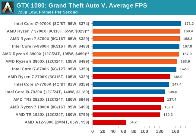 |
|
 |
 |
| 95th Percentile | 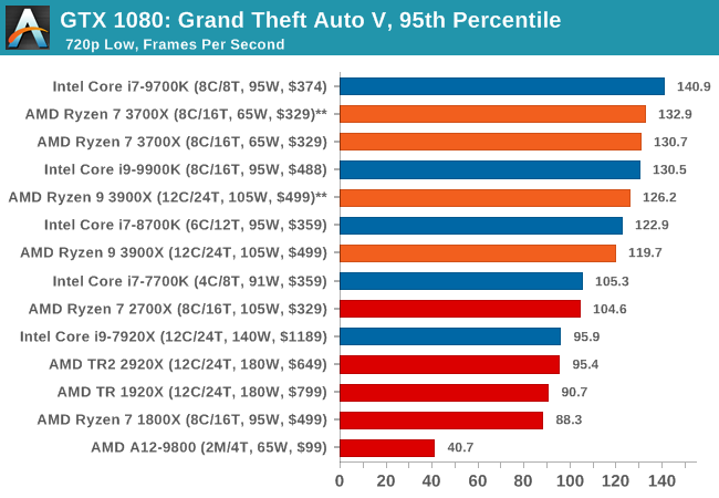 |
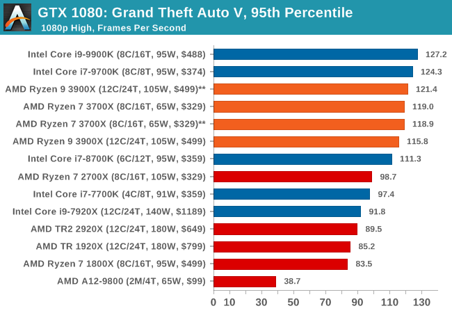 |
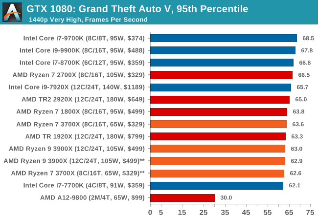 |
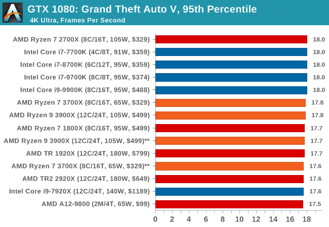 |
Aside from keeping up-to-date on the Formula One world, F1 2017 added HDR support, which F1 2018 has maintained; otherwise, we should see any newer versions of Codemasters' EGO engine find its way into F1. Graphically demanding in its own right, F1 2018 keeps a useful racing-type graphics workload in our benchmarks.
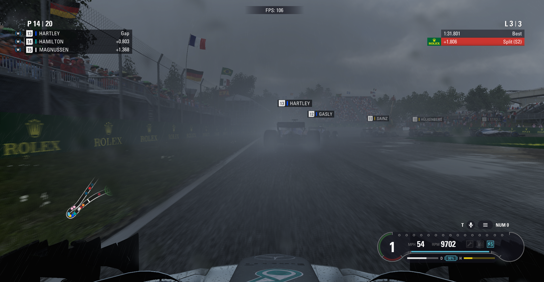
Aside from keeping up-to-date on the Formula One world, F1 2017 added HDR support, which F1 2018 has maintained. We use the in-game benchmark, set to run on the Montreal track in the wet, driving as Lewis Hamilton from last place on the grid. Data is taken over a one-lap race.
| AnandTech CPU Gaming 2019 Game List | ||||||||
| Game | Genre | Release Date | API | IGP | Low | Med | High | |
| F1 2018 | Racing | Aug 2018 |
DX11 | 720p Low |
1080p Med |
4K High |
4K Ultra |
|
All of our benchmark results can also be found in our benchmark engine, Bench.
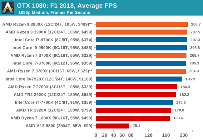
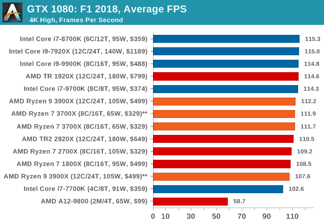
| F1 2018 | IGP | Low | Medium | High |
| Average FPS | 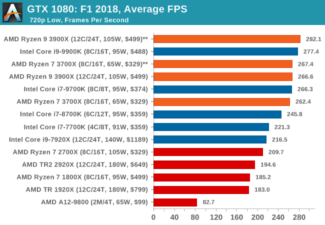 |
|
 |
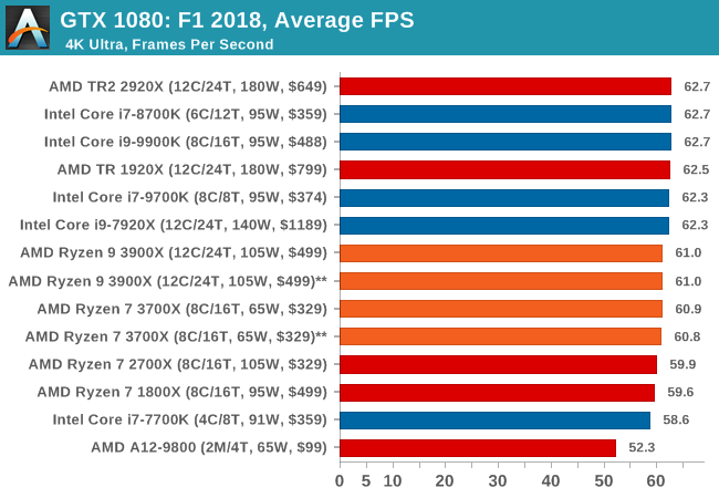 |
| 95th Percentile | 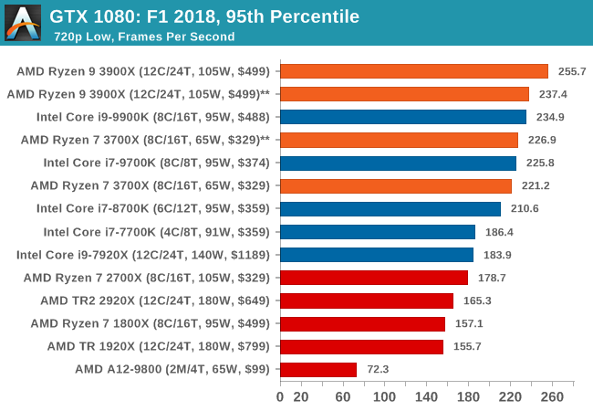 |
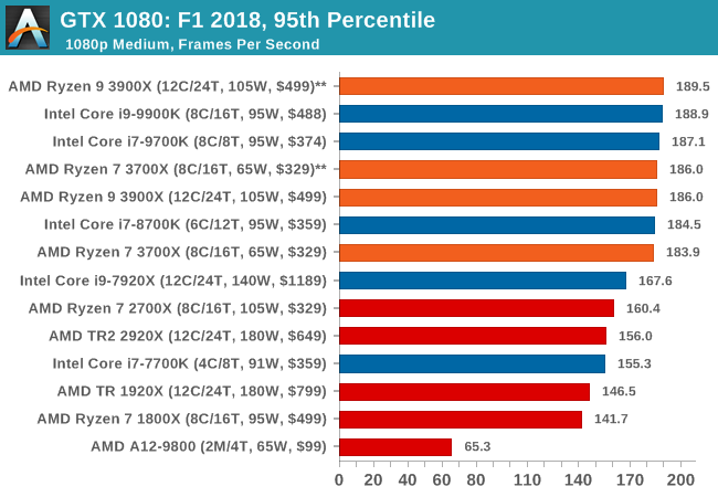 |
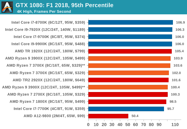 |
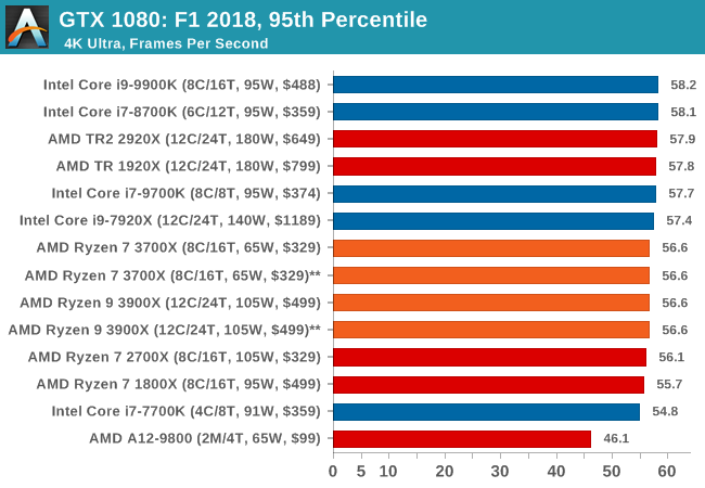 |
Power consumption of the new Ryzen 3900 and 3700X are of particular interest because it’s a very key aspect of the new generation chipsets, and AMD promises some extremely large improvements thanks to the new 7nm process node as well as the optimised chiplet design.
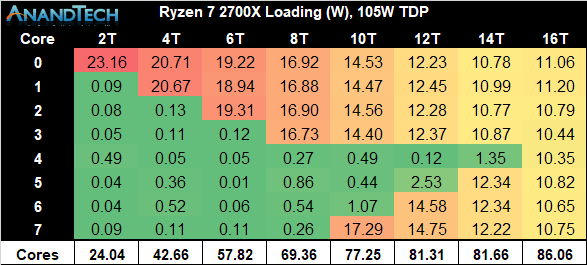
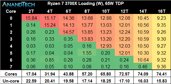
When comparing the single-chiplet Ryzen 3700X to the previous generation Ryzen 2700X, we’re seeing quite some dramatic differences in core power consumption. In particular power consumption at each chip’s respective peak frequency is notably different: Although the new 3700X has a 100MHz higher clock speed and thus is further up the exponential power curve, it manages to showcase 32% lower absolute power than the 2700X.
We have to remember that we’re talking about overall absolute power, and not efficiency of the chip. When taking actual performance into account through the higher clock as well as Zen2’s increased performance per clock, the Performance/W figures for the new 3700X should be significantly higher than its predecessor.
What is curious about the new chip is just how closely it follows its power limitations. The new boosting algorithm on the Ryzen 3 series is a particularly “opportunistic” one that will go as high in frequencies as it can go within its constraints, no matter the amount of CPU cores.
The constraints are as follows:
- Package Power Tracking (PPT): The power threshold that is allowed to be delivered to the socket.
- This is 88W for 65W TDP processors, and 142W for 105W TDP processors.
- Thermal Design Current (TDC): The maximum amount of current delivered by the motherboard’s voltage regulators when under thermally constrained scenarios (high temperatures)
- This is 60A for 65W TDP processors, and 95A for 105W TDP processors.
- Electrical Design Current (EDC): This is the maximum amount of current at any instantaneous short period of time that can be delivered by the motherboard’s voltage regulators.
- This is 90A for 65W TDP processors, and 140A for 105W TDP processors.
Looking at the total power consumption of the new 3700X, the chip is very much seemingly hitting and maintaining the 88W PPT limitations of the default settings, and we’re measuring 90W peak consumption across the package.
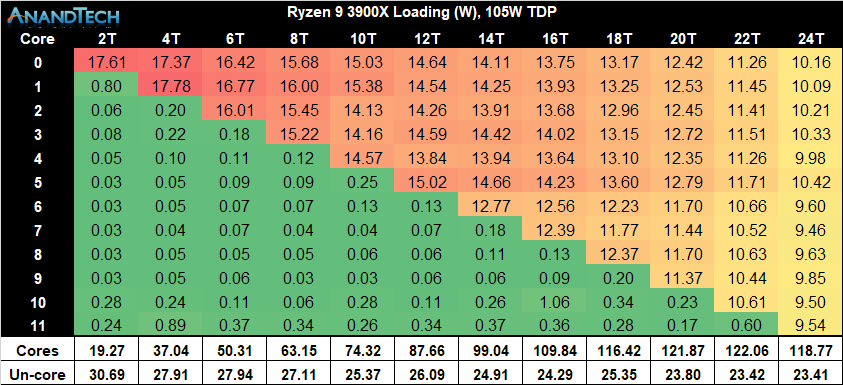
When having a closer look at the new Ryzen 9 3900X, first we have to enjoy the sheer amount of cores of this processor!
Following that, we see that this CPU’s per-core peak power consumption is quite notably higher than that of the 3700X, which is not a surprise given that the chip is clocked 200MHz higher at 4.6GHz versus “just” 4.4GHz. However even at this much higher clock, the 3900X’s power consumption remains notably lower than that of the 2700X.
Scaling up in threads as well as cores, we’re seeing a similar scaling behaviour, with the large difference being that the 3900X is maintaining higher power consumption per core (and frequency) than the 3700X. Fully loading the chip we’re seeing 118W power on the CPU cores while the package power is falling in at the exact 142W that AMD describes as the PPT limit of 105W TDP processors such as the 3900X.
Another thing to note in the results between the 3700X results and the 3900X, is that un-core power on the latter is quite higher. This really shouldn’t come as a surprise as the processor has a second chiplet who will have L3 and Infinity Fabric that will use more power.
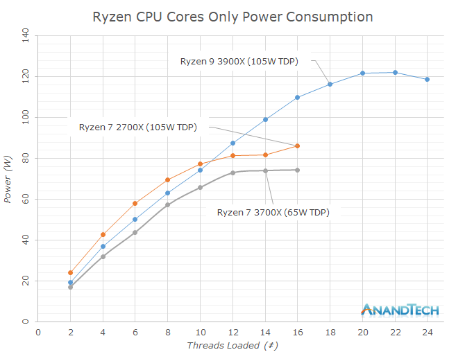
Graphing the three processors together, we see two main aspects: Again the 3900X and 3700X both consuming notably less power than the 2700X, and the 3700X’s hard limit when reaching the 88W PPT limit while the 3900X is able to scale further up till it hits the 142W limit.
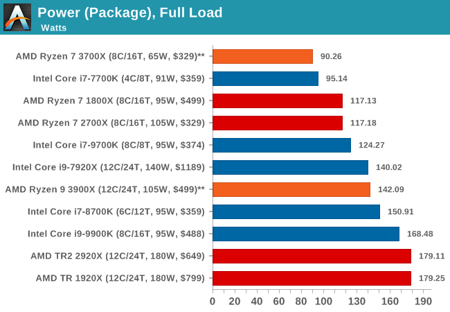
Comparing the full load power characteristics of both SKUs, they end up extremely competitive in both their respective categories. The 3700X’s 90W hard-limit puts it at the very bottom of the CPUs we’ve used in our testing today, which is quite astonishing as the chip is trading blows with the 9700K and 9900K across all of our test workloads, and the latter chip’s power consumption is well over 60% above the 3700X’s.
The 3900X is also impressive given that it’s a 12-core CPU. While posting substantial performance improvements of the 12-core Threadripper counterparts, the 3900X still manages to be significantly less thermally constrained thanks to its much lower power consumption, peaking in at 142W.
The most interesting aspect of AMD’s new opportunistic power boost mechanism lies in a CPU we weren’t able to test today: the Ryzen 7 3800X. At stock behaviour, the chip’s 105W TDP should allow it to behave a lot more like the 3900X when it comes to the higher thread-count frequencies, at least until it maxes out its 8 cores on its single chiplet, which might really put it ahead of the 3700X in terms of multi-threaded performance workloads.
Overclocking: PBO & All-Core
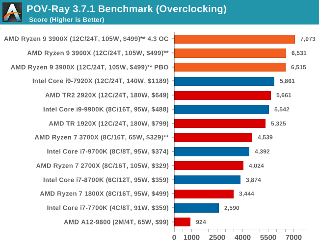
In POV-Ray, running the 3900X at a flat 4.3GHz gives it a 8.2% performance boost over stock. Enabling PBO doesn’t make much difference in multi-threaded workloads for the 3900X as it’s still being limited by the 142W PPT limit.
Unfortunately we weren’t able to further investigate raising the PPT limit for this article due to time contraints as well as currently non-final firmware version for X570 motherboards from the vendors.
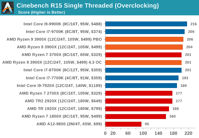
Turning on PBO will increase the single-threaded performance of the 3900X by a few percent, scoring just slightly higher than the stock settings. Naturally the 4.3 GHz flat overclock will regress in performance as it loses out 300MHz peak frequency compared to stock.
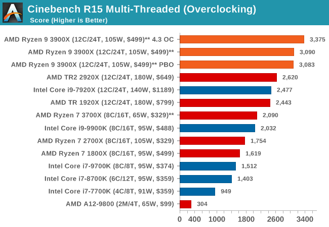
Finally, a Cinebench R15 MT run shows similar multi-threaded behaviour, with the 4.3GHz flat overclock achieving a 9.2% better score, whilst the PBO overclock isn’t able to further increase frequencies beyond the default power limits of the chip.
Overall, we’ve been eagerly awaiting today’s launch for months, and all the while AMD has certainly given us some high expectations for their 3rd generation Ryzen CPUs. At the end of the day I think that AMD was able to deliver on all of their promises, and hitting all of the performance targets that they needed to. Furthermore, where AMD kills it is in terms of value, as both the 3700X and the 3900X really deliver in terms of offering outstanding alternatives to the competition.
The New Zen 2 µarch & Chiplet Design
The basis for the new 3rd generation Ryzen processors is AMD’s new high-risk high-reward bet on moving away from a single monolithic die to a chiplet-based MCM (Multi-chip module) design. What this has allowed AMD to do is to maximise the performance characteristics of their 7nm design for the new Ryzen 3000 chipsets. Meanwhile, having the I/O components and the memory controllers on a 12nm process node not only allows AMD to minimise the cost of the platform, but also allows them to optimise the silicon for their specific use-cases.
The actual CPU chiplets (CPU-lets?) are manufactured on TSMC’s leading edge 7nm process node and AMD has seemingly been able to take full advantage of the process, not only lowering the power consumption of the cores, but actually also raising the clock frequency at the same time, bringing for some impressive power efficiency benefits.
The new design did seemingly make some compromises, and we saw that the DRAM memory latency of this new system architecture is slower than the previous monolithic implementation. However, here is also where things get interesting. Even though this is a theoretical regression on paper, when it comes to actual performance in workloads the regression is essentially non-existent, and AMD is able to showcase improvements even in the most memory-sensitive workloads. This is thanks to the new Zen 2 CPU core’s improved microarchitecture, with new improved prefetchers and overall outstanding Memory Level Parallelism (MLP) designs. Further helping AMD's memory/cache situation is the doubling of the CCX’s L3 cache from 8MB to 16MB, which on average, ends up with better workload memory performance.
Not that Zen 2 is soley about memory performance, either. The CPU core's front-end improvements such as the new TAGE predictor – and in particular the much increased capacity of the operation cache – is very visible in some workloads. We’ve also seen the core’s new 256-bit (AVX2) vector datapaths to work very well.
In the majority of controlled tests, AMD has done something they haven’t been able to achieve in almost 15 years, since the tail-end of the Athlon 64's reign in 2005: that is to have a CPU microarchitecture with higher performance per clock than Intel's leading architecture. Zen 2 finally achieves this symbolic mark by a hair’s margin, with the new core improving IPC by 10-13% when compared to Zen+.
Having said that, Intel still very much holds the single-threaded performance crown by a few percent. Intel’s higher achieved frequencies as well as continued larger lead in memory sensitive workloads are still goals that AMD has to work towards to, and future Zen iterations will have to further improve in order to have a shot at the ST performance crown.
Beyond this, it’s remarkable that AMD has been able to achieve all of this while having significantly lower power consumption than Intel's best desktop chip, all thanks to the new process node.

The 3700X & 3900X Versus The Competition, Verdict
Office CPU Performance and Productivity
It’s in these categories where AMD’s strengths lie: In the majority of our systems benchmarks, AMD more often than not is able to lead Intel’s 9700K and 9900K in terms of performance. Particularly it was interesting to see the new 3rd gen Ryzens post larger improvements in the web tests, all thanks to Zen 2’s improved and larger op cache.
In anything that is remotely multi-threaded, AMD is also able to take the performance crown, with only Intel’s HEDT i9-7920X being able to top the new 12-core Ryzen 3900X. The 3700X here still hangs in there being extremely competitive, falling in-between the 9700K and 9900K when it comes to multi-threaded workloads, sometimes even beating the 9900K in some workloads, a respectable result.
Gaming Performance
When it comes to gaming performance, the 9700K and 9900K remain the best performing CPUs on the market.
That being said, the new 3700X and 3900X are posting enormous improvements over the 2700X, and we can confirm AMD’s claims of up to 30-35% better performance in some games over the 2700X.
Here’s the thing: while AMD does still lag behind Intel in gaming performance, the gap has narrowed immensely to the point that the Ryzen CPUs are no longer something to be dismissed if you want to have a high-end gaming machine, and are still very much a viable option worth considering.
Everything Tied Together: A Win For AMD
What really does make the Ryzen 3700X and 3900X winners in my eyes is their overall packages and performance. They’re outstanding all-rounders and AMD has managed to vastly improve some of the aspects it was lagging behind the most. Whilst AMD has to further push single-threaded performance in the future and continue working on improving memory performance, they’re on Intel’s tail.
The big argument for the 3700X and 3900X is their value as well as their power efficiency. At $329 the 3700X particularly seems exciting and posts near the same gaming performance as the 3900X at $499. Considering that AMD is also shipping the CPU with a viable Wrath Spire, this also adds on to the value that you get if you’re budget conscious.
The 3900X essentially has no competition when it comes to the multi-threaded performance that it’s able to deliver. Here the chip not only bests Intel’s designs, which is able to go toe-to-toe only with >$1500 HEDT platforms, but also suddenly makes AMD’s own Threadripper line-up quite irrelevant.
All in all, while AMD still has some ways to go, they’ve never been this close to Intel in over a decade, and if the company is able to continue to execute as well, we should be seeing exciting things in the future.
https://www.anandtech.com/show/14605/the-ryzen-3700x-3900x-review-raising-the-bar
2019-07-07 13:05:22Z
52780327326446


